
Chunmeng Li, Xiaoqiang Chen, Ying Wang. Study on Rhombic Slot Antenna at Ridge Edge of Single Ridge Waveguide[J]. Laser & Optoelectronics Progress, 2021, 58(5): 0523001
- Laser & Optoelectronics Progress
- Vol. 58, Issue 5, 0523001 (2021)
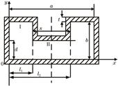
Fig. 1. Schematic diagram of the cross section of the single ridge waveguide
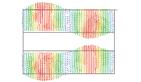
Fig. 2. Ridge edge current distribution of the single ridge waveguide
Fig. 3. Current distribution on the narrow side of the rectangular waveguide
Fig. 4. Schematic diagram of the double slot at ridge edge
Fig. 5. VSWR corresponding to different slot width
Fig. 6. Resonant cutting depth corresponding to different slot width
Fig. 7. VSWR corresponding to different wall thickness
Fig. 8. Resonant cutting depth corresponding to different wall thickness
Fig. 9. VSWR corresponding to different b/a
Fig. 10. Resonance cutting depth corresponding to different b/a
Fig. 11. VSWR corresponding to different s/a
Fig. 12. Resonant cutting depth corresponding to different s/a
Fig. 13. VSWR corresponding to different e/b
Fig. 14. Resonant cutting depth corresponding to different e/b
Fig. 15. VSWR corresponding to different width sides
Fig. 16. Resonant cutting depth corresponding to different wide side
Fig. 17. Current excitation distribution of the slot
Fig. 18. Theoretical conductance distribution of the slot
Fig. 19. Relationship between conductance and dip angle
Fig. 20. Radiation pattern of main polarization and cross polarization of rhombic slot antenna at the ridge edge of the single ridge waveguide
|
Table 1. Angle and resonant cutting depth of each gap
|
Table 2. Comparison of the cross polarization level

Set citation alerts for the article
Please enter your email address
© Copyright 2018-2021 | Chinese Laser Press. All Rights Reserved 沪ICP备15018463号-20