• Journal of Infrared and Millimeter Waves
  • Vol. 41, Issue 2, 384 (2022)
Lu-Hong WAN1、2、3, Xiu-Mei SHAO1、2、*, Xue LI1、2、**, Yi GU1、2, Ying-Jie MA1、2, and Tao LI1、2
Author Affiliations
  • 1State Key Laboratories of Transducer Technology,Shanghai Institute of Technical Physics,Chinese Academy of Sciences,Shanghai 200083,China
  • 2Key Laboratory of Infrared Imaging Materials and Detectors,Shanghai Institute of Technical Physics,Chinese Academy of Sciences,Shanghai 200083,China
  • 3University of Chinese Academy of Sciences,Beijing 100049,China
  • show less
    DOI: 10.11972/j.issn.1001-9014.2022.02.002 Cite this Article
    Lu-Hong WAN, Xiu-Mei SHAO, Xue LI, Yi GU, Ying-Jie MA, Tao LI. Interfacial properties between Al2O3 and In0.74Al0.26As epitaxial layer on MIS capacitors[J]. Journal of Infrared and Millimeter Waves, 2022, 41(2): 384 Copy Citation Text show less

    Abstract

    Metal-Insulator-Semiconductor (MIS) capacitors were fabricated on In0.74Al0.26As/In0.74Ga0.26As/InxAl1-xAs heterostructure multilayer semiconductor materials. SiNx and SiNx/Al2O3 bilayer were applied as insulating layer to prepare MIS capacitors respectively. High-resolution transmission electron microscopy (HRTEM) and X-ray photoelectron spectroscopy (XPS) measurements indicated that, compared with SiNx deposited by inductively coupled plasma chemical vapor deposition (ICPCVD), Al2O3 deposited by atomic layer deposition (ALD) can effectively suppresses In2O3 at the interface between Al2O3 and In0.74Al0.26As. According to the capacitance-voltage (C-V) measurement result of MIS capacitors, the fast interface state density (Dit) of SiNx/Al2O3/In0.74Al0.26As was one order of magnitude lower than that of SiNx/In0.74Al0.26As. Therefore, it can be concluded that Al2O3 deposited by ALD as a passivation film can effectively reduce the interface state density between Al2O3 and In0.74Al0.26As, thereby reducing the dark current of p-In0.74Al0.26As/i-In0.76Ga0.24As/n-InxAl1-xAs photodiodes.

    Introduction

    InGaAs photodiodes are very promising and have been widely used in short wavelength infrared(SWIR)detection 1-2. The defects caused by the lattice mismatch between In0.74Ga0.26As and InP substrate is inevitable. In order to improve the performance of In0.74Ga0.26As photodiodes,it is necessary to optimize the epilayer and manufacturing processes of the InGaAs photodiodes. The dark current of the mesa In0.74Ga0.26As photodiodes is composed of body dark current and side dark current 3. Passivation is one of the key processes of the mesa PIN photodiodes. Therefore,it is essential to optimize the passivation to reduce the dark current of the mesa In0.74Al0.26As(p)/In0.74Ga0.26As(i)/InxAl1-xAs(n)photodiodes.

    As an outstanding thin film deposition technology,ALD has broad prospects in semiconductor device fabrication 4-6. ALD involves two self-limiting surface reactions in which the growth substrate is exposed to alternating pulses of co-reactant and precursor 7-8. Therefore,ALD can precisely control the thickness of thin film with an accuracy of an atomic layer. Moreover,films deposited by ALD are dense and of high quality. In our previous work,Al2O3 deposited by ALD has been proved to be an effective passivation film in In0.74Ga0.26As photodiodes 9-10. However,the reason why the ALD-Al2O3 reduces the dark current of In0.74Ga0.26As photodiodes has not been explored. Therefore,it is necessary to study the interface state density between ALD-Al2O3 and In0.74Al0.26As layer.

    In this paper,TEM and XPS measurements were performed to investigate the interface between two different dielectric films and In0.74Al0.26As layer. The two different dielectric films were ALD-Al2O3 and ICPCVD-SiNx respectively. In addition,MIS capacitors have been prepared by using above two dielectric films to further quantitatively study the interface state density between dielectric film and In0.74Al0.26As layer.

    1 Experimental details

    To investigate the interface state density of SiNx/In0.74Al0.26As and SiNx/Al2O3/ In0.74Al0.26As,two series of MIS capacitor were prepared. The SiNx or Al2O3 were deposited on the In0.74Al0.26As/In0.74Ga0.26As/InxAl1-xAs heterostructures that were grown on an InP substrate by gas source molecular beam epitaxy(MBE)11. What’s more,the materials used to prepare the samples were cleaved from the same wafer. To remove surface native oxide layer,the wafer involved in this paper were treated with hydrofluoric acid buffer solution before film deposition.

    TEM and XPS measurements were employed to investigate the interface between films and In0.74Al0.26As layer. The 20-nm-thick Al2O3 films were deposited on In0.74Al0.26As by 220 cycles of trimethylaluminum(TMA)and H2O at 150°C for the TEM and XPS measurements. For comparison purpose,about 20-nm-thick SiNx films were deposited on In0.74Al0.26As by ICPCVD of SiH4 and N2 at 75°C for the TEM and XPS measurements. Furthermore,bare In0.74Al0.26As wafer with native oxides was used as a control for XPS measurement. The insulator of sample A was deposited with 135-nm-thick SiNx film by ICPCVD. The insulator of sample B is ICPCVD-SiNx/ALD-Al2O3 bilayer,where 20-nm-thick Al2O3 was firstly deposited by ALD and 130-nm-thick SiNx was then deposited by ICPCVD.
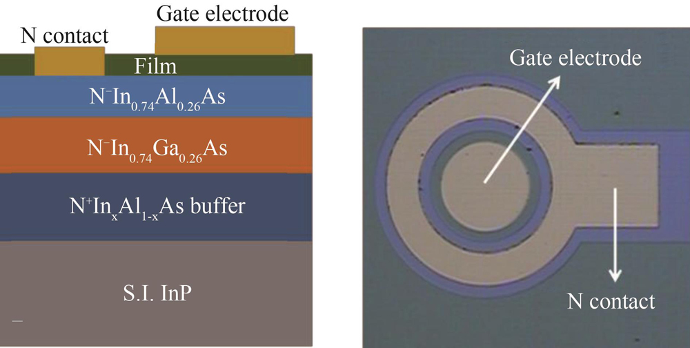
 Fig. 1(a)shows the sectional schematic of MIS capacitors. The dielectric film of sample A and sample B were SiNx film and SiNx/Al2O3 bilayer respectively. The photography of MIS capacitor was represented in Fig. 1(b). The C-V characteristics of MIS capacitors at different frequencies were measured by Agilent B1500A Semiconductor Device Analyzer.

    (a)Sectional schematic diagram and(b)photography of MIS capacitor

    Figure 1.(a)Sectional schematic diagram and(b)photography of MIS capacitor

    2 Results and discussion

    Pt was firstly deposited on the surface of In0.74Al0.26As wafer to protect the wafer from etching damage. Focused Ion Beam(FIB)was used to thin the sample,and then the thinned sample was subjected to TEM testing. The cross-section TEM images of ICPCVD-SiNx/In0.74Al0.26As and ALD-Al2O3/In0.74Al0.26As structure were shown in Fig. 2(top). In comparison with SiNx/In0.74Al0.26As,a sharp transition from Al2O3 to In0.74Al0.26As can be observed. In addition,the cross-sectional composition information of Fig. 2(bottom)obtained by Energy Dispersive X-ray Spectroscopy(EDS)can also illustrate this. The transition from SiNx to In0.74Al0.26As layer was ~5 nm,while the transition from Al2O3 to In0.74Al0.26As layer was ~3 nm.

    The cross-sectional images(top)obtained by TEM and cross-sectional composition information(bottom)obtained by EDS of(a)ICPCVD-SiNx on In0.74Al0.26As and(b)ALD-Al2O3 on In0.74Al0.26As

    Figure 2.The cross-sectional images(top)obtained by TEM and cross-sectional composition information(bottom)obtained by EDS of(a)ICPCVD-SiNx on In0.74Al0.26As and(b)ALD-Al2O3 on In0.74Al0.26As

    In order to further study the interface state density between film and In0.74Al0.26As,XPS test combined with Ar+ sputtering(2 kV,20 μA)was utilized. XPS spectra were obtained with the Axis UltraDLD spectrometer(Kratos Analytical-A Shimadzu Group Company)with a monochromatic Al Kα source(=1486.6 eV)and a charge neutralization system. The spectra were taken when the vacuum of the analysis chamber was less than 5×10⁻⁹ Torr. The electron energy analyzer works in the hybrid magnification mode,and the take-off angle for the analyzer relative to sample surface is 90°. The X-ray source power was set to 105 W(15 kV,7 mA)for high-resolution spectra acquisition. The pass energy of 40 eV were utilized for narrow scan spectra. The energy step size of 0.1 eV were chosen for narrow scan spectra. The C 1s peak of environmental pollution carbon adsorbed on the sample surface is used as the reference peak for spectral energy correction to complete the peak position calibration:set the C 1s peak position of the pollution carbon to 284.8 eV. Calculate the relative percentage of elements through the peak area of the element peak and the sensitivity factor of the instrument.

    In3d5/2 spectra obtained by XPS narrow scan was shown in Fig. 3. As shown in Fig. 3(a),there was a certain amount of In2O3 on the surface of the bare In0.74Al0.26As wafer. Compared with the surface of bare In0.74Al0.26As wafer,almost no In2O3 could be found in the bulk of In0.74Al0.26As[Fig. 3(b)]. The amount of In2O3 at the SiNx/In0.74Al0.26As interface[Fig. 3(e)]was less than that of the surface of bare In0.74Al0.26As wafer. However,there was still a certain amount of In2O3 at the SiNx/In0.74Al0.26As interface that couldn’t be ignored. Thus,ICPCVD-SiNx film could reduce part of In2O3 at the interface between SiNx and In0.74Al0.26As. The interface between Al2O3/In0.74Al0.26As[Fig. 3(h)]was equivalent to the bulk of In0.74Al0.26As,and there was almost no In2O3 could be found at the interface between Al2O3 and In0.74Al0.26As. Therefore,it can be concluded that ALD-Al2O3 can effectively suppress the In2O3 at the interface between film and In0.74Al0.26As.

    The 3d5/2 core level of In recorded from bare In0.74Al0.26As wafer,ICPCVD-SiNx/In0.74Al0.26As and ALD-Al2O3/In0.74Al0.26As(a)on the surface of bare In0.74Al0.26As,(b)in the bulk of In0.74Al0.26As,(c)on the surface of ICPCVD-SiNx,(d)in the bulk of ICPCVD-SiNx,(e)at the interface between ICPCVD-SiNx and In0.74Al0.26As,(f)on the surface of ALD-Al2O3,(g)in the bulk of ALD-Al2O3,and(h)at the interface between ALD-Al2O3 and In0.74Al0.26As

    Figure 3.The 3d5/2 core level of In recorded from bare In0.74Al0.26As wafer,ICPCVD-SiNx/In0.74Al0.26As and ALD-Al2O3/In0.74Al0.26As(a)on the surface of bare In0.74Al0.26As,(b)in the bulk of In0.74Al0.26As,(c)on the surface of ICPCVD-SiNx,(d)in the bulk of ICPCVD-SiNx,(e)at the interface between ICPCVD-SiNx and In0.74Al0.26As,(f)on the surface of ALD-Al2O3,(g)in the bulk of ALD-Al2O3,and(h)at the interface between ALD-Al2O3 and In0.74Al0.26As

    Figure 4 shows the C-V curves of SiNx/In0.74Al0.26As and SiNx/Al2O3/In0.74Al0.26As MIS capacitors with bias voltage from 25 V to -25 V at 210 K. The C-V measurements of these capacitors was performed with frequency varying from 1 kHz to 1 MHz. Under the low frequency limit,the capacitance of MIS capacitor(CLF)was equivalent to the parallel connection of semiconductor capacitance(Cs)and interface trap capacitance(Cit)and then the series connection of insulating layer capacitance(Ci). Therefore,the CLF can be expressed as:

    1CLF=1Cs+Cit+1Ci .

    C-V curves of MIS capacitors measured at 210 K for different frequencies from 1 kHz to 1 MHz(a)SiNx/In0.74Al0.26As MIS capacitor,(b)SiNx/Al2O3 In0.74Al0.26As MIS capacitor

    Figure 4.C-V curves of MIS capacitors measured at 210 K for different frequencies from 1 kHz to 1 MHz(a)SiNx/In0.74Al0.26As MIS capacitor,(b)SiNx/Al2O3 In0.74Al0.26As MIS capacitor

    However,under the high frequency limit,the interface trapped charge can not keep up with the change of high frequency. Therefore,the capacitance of MIS capacitor(CHF)was equivalent to the series connection of semiconductor capacitance(Cs)and insulating layer capacitance(Ci). Thus,the CHF can be expressed as:

    1CHF=1Cs+1Ci .

    According to Eqs(1-2),the fast interface state density(Dit)can be expressed as(high-low frequency method)12-13

    Dit=Citq2=CiqA(CLFCi-CLF-CHFCi-CHF)

    where A is the area of gate electrode.

    In this paper,the CLF was the capacitance of MIS capacitor under 1 kHz,while the CHF was the capacitance of MIS capacitor under 1 MHz. The Dit values of sample A and B were 2.29×1013 cm-2eV-1 and 1.83×1012 cm-2eV-1 respectively,which were calculated by high-low frequency method. Apparently,the calculated Dit of sample B is an order of magnitude smaller than that of sample A. Thus,ALD-Al2O3 effectively reduces the Dit between Al2O3 and In0.74Al0.26As. This can be explained by the growth of Al2O3 deposited by ALD. Firstly,an aluminum source is introduced to effectively neutralize the dangling bonds on the surface of In0.74Al0.26As,and then a water source is introduced to form a bond with aluminum. Therefore,the interface state density(such as In2O3)between the dielectric film and In0.74Al0.26As is effectively reduced.

    Combining the XPS test and the C-V measurement results of the MIS capacitors,it can be concluded that ALD-Al2O3 effectively reduces the fast interface state density between the film and the In0.74Al0.26As. Therefore,the lower 1/f noise and dark current density characteristics of In0.74Ga0.26As photodiodes passivated by SiNx/Al2O3 bilayer 9-10are attributed to the lower fast interface state density between the film and the In0.74Al0.26As.

    3 Conclusion

    According to the study of the interface between dielectric film and In0.74Al0.26As,it is found that the interface between the ALD-Al2O3 and In0.74Al0.26As is sharper than that of ICPCVD-SiNx and In0.74Al0.26As. In addition,ALD-Al2O3 effectively reduces the In2O3 at the interface between ALD-Al2O3 and In0.74Al0.26As. Furthermore,the C-V results of the MIS capacitors also indicate that the ALD-Al2O3 effectively reduces the fast interface state density of the dielectric film and In0.74Al0.26As. In summary,using ALD-Al2O3 as the passivation film of the In0.74Ga0.26As photodiodes can theoretically reduce the dark current of the In0.74Ga0.26As photodiodes. Furthermore,the device verification results have confirmed this statement.

    References

    [1] C Huang, C L Ho, M C Wu. Large-area planar wavelength extended InGaAs p-i-n photodiodes using rapid thermal diffusion with spin-on dopant technique. IEEE Electron Device Lett, 36, 820-822(2015).

    [2] X Li, H Gong, J X Fang et al. The development of InGaAs short wavelength infrared focal plane arrays with high performance. Infrared Physics and Technol, 80, 112-119(2017).

    [3] A Rouvié, J L Reverchon, O Huet et al. InGaAs focal plane array developments at III-V Lab. Proc. SPIE, 8353, 835308(2012).

    [4] O Sneh, R B Clark-Phelps, A R Londergan et al. Thin film atomic layer deposition equipment for semiconductor processing. Thin Solid Films, 402, 248-261(2002).

    [5] A F Palmstrom, P K Santra, S F Bent. Atomic layer deposition in nanostructured photovoltaics: Tuning optical, electronic and surface properties. Nanoscale, 7, 12266-12283(2015).

    [6] N P Dasgupta, X B Meng, J W Elam et al. Atomic layer deposition of metal sulfide materials. Acc. Chem. Res, 48, 341-348(2015).

    [7] L Zhou, B X Bo, X Z Yan et al. Brief review of surface passivation on III-V semiconductor. Crystals, 8, 226(2018).

    [8] M Leskela, M Mattinen, M Ritala. Review Article Atomic layer deposition of optoelectronic materials. J. Vac. Sci. Technol. B, 37, 030801(2019).

    [9] L H Wan, G Q Cao, X M Shao et al. High performance In0.83Ga0.17As SWIR photodiode passivated by Al2O3/SiNx stacks with low-stress SiNx films. J. Appl. Phys, 126, 033101(2019).

    [10] L H Wan, X M Shao, Y J Ma et al. Dark current and 1/f noise characteristics of In0.74Ga0.26As photodiode passivated by SiNx/Al2O3 bilayer. Infrared Physics and Technol, 109, 103389(2020).

    [11] Y G Zhang, Y Gu, C Zhu et al. Gas source MBE grown wavelength extended 2.2 and 2.5 μm InGaAs PIN photodetectors. Infrared Phys. Technol, 47, 257-262(2006).

    [12] R Engel-Herbert, Y Hwang, S Stemmer. Comparison of methods to quantify interface trap densities at dielectric/III-V semiconductor interfaces. J. Appl. Phys, 108, 124101(2010).

    [13] R Castagné, A Vapaille. Description of the SiO2-Si interface properties by means of vary low frequency MOS capacitance measurements. Surf. Sci, 28, 157(1971).

    Lu-Hong WAN, Xiu-Mei SHAO, Xue LI, Yi GU, Ying-Jie MA, Tao LI. Interfacial properties between Al2O3 and In0.74Al0.26As epitaxial layer on MIS capacitors[J]. Journal of Infrared and Millimeter Waves, 2022, 41(2): 384
    Download Citation