Ping Xie, Bin Li, Suying Zhang, Dingquan Liu, "Using lead germanium telluride as a high-index coating material in the mid-wavelength infrared narrow bandpass filters," Chin. Opt. Lett. 13, 123101 (2015)
Copy Citation Text
In our investigation, lead germanium telluride, which is a pseudo-binary alloy of IV-VI narrow-gap semiconductor compounds of PbTe and GeTe, can be used in the fabrication of mid-wavelength infrared narrow bandpass filters as a high-index coating material, due to its high refractive index, lower absorption, and tunability of fundamental absorption edges. It is demonstrated that a half-width of 160 nm and a better rejection ratio can be obtained for a simple 8-layer double cavity filter with a central wavelength at 4 μm, compared with a half-width of 390 nm for those conveniently fabricated using Ge as high-index material.
The rapid detection of dynamites or explosives is of increasing importance in the anti-terror campaign. A technology to detect trace dynamites can be developed using electromagnetic radiation in the mid-wavelength infrared region, preferably in the range between 3–5 μm, because many strong fundamental absorption bands, termed as fingerprint, emerge in this range. Although in recent years significant progress has been made toward the miniaturization of infrared spectrometers for homeland security and law enforcement applications due to the development of thermoelectrically cooled detectors and quantum cascade lasers, a thin-film narrowband transmission filter is urgently needed with a passband coinciding with and as narrow as the typical absorption line at atmospheric pressure to increase the sensitivities of the instruments. If the characteristic lines assigned to the trace dynamites can be distinguished by a thin-film interference filter, which has an order of magnitude larger angular dispersion than gratings, the spectral fluctuation will be reduced considerably and a greater level of miniaturization can be completely achieved without clumsy gratings. Furthermore, more profits can be gained out of the mass production of thin-film filters.
According to Macleod[1], the simplest type of one-cavity all-dielectric Fabry–Perot filter has the form of or , where and are quarter-wavelength layers with high and low refractive indices, respectively, is the order of the spacer, and is the number of full periods in the reflecting stacks. The expressions for its half-width are for the high-refractive-index spacer, and for the low-refractive-index spacer, where being the central wavelength, and , , and are the indices of refraction of the high-index layers, low-index layers in the filter, and the substrate, respectively. Therefore, in order to reduce the half-width of a Fabry–Perot filter, accompanied by increasing the number of full periods in the reflecting stacks and the order of interference of the spacer, it is almost always advantageous to use the highest and lowest indices available for all dielectric layers in the spectral regions of interest. The greater the value of is, the narrower the half-width can be obtained.
Conveniently, germanium (Ge) and either silicon monoxide (SiO) or silicon dioxide are the preferred choices for the high and low index extremes in the spectral region of mid-wavelength infrared. Ge has a high index round 4.0 in the spectral range from 2 μm to at least 14 μm. However, it can be expected that the half-width of a filter will be further reduced if another material with an even higher index available to substitute for Ge.
Sign up for Chinese Optics Letters TOC. Get the latest issue of Chinese Optics Letters delivered right to you!Sign up now
Lead telluride (PbTe), one of the lead chalcogenides used in thermoelectricity and infrared detection, is also one of high index infrared coating materials. Currently, it dominates the material selection for the design of infrared interference filters operating in the long wavelength infrared both at room and reduced temperatures. The combination of its high index (above 5.5 in the spectral range of long-wavelength infrared at room temperature), and its advantage of a negative temperature coefficient of refractive index , make it much superior to other infrared coating materials[2–5]. However, it is as transparent as a thin-film material until 3.8 μm; therefore, the position of the fundamental absorption edge is hindering it from being used in the spectral region of mid-wavelength infrared.
Lead germanium telluride is a pseudo-binary alloy of IV-VI narrow-gap semiconductor compounds, PbTe, and GeTe[6–11]. In our investigations, it can be demonstrated that the absorption edges of the thin films of can be tuned toward short wavelengths by increasing the Ge concentration. Therefore, an attempt can be made to construct a thin-film narrow bandpass filter operating in the spectral range of mid-wavelength infrared using as a high-index material to substitute for Ge.
The starting materials of with different Ge concentration , 0.08, 0.10, 0.12, 0.14, 0.16, 0.17, and 0.25, were synthesized from Pb, Ge, and Te with a purity of 99.9999% in a slight excess of Te proportion , respectively. Syntheses were carried out at 1100°C in evacuated silica ampoules, of which the inside surfaces were pyrolized with carbon to avoid the reaction of lead with silica. After the process of syntheses, the resulting ingots were held at 700°C for 24 h, then cooled down to room temperature at a rate of 10°C/h. Subsequently, the ingots were crushed into small pieces with an approximate size of 5 mm and used as evaporants.
The evaporants of were evaporated to deposited thin films using molybdenum boats in a KD500 box coater with a background vacuum of . A flat calotte rotated at a rate of 30 rpm to provide a good uniformity of thin films. Double-sided polished single-crystal silicon (100) wafers with a diameter of 10 mm and a thickness of 0.8 mm were used as substrates, which were heated by radiation heaters. The substrate temperature was sensed by platinum resistance temperature transducers. The signals from the transducers were transferred out through a set of electric brushes and slip rings to operate a temperature controller and thus maintained a constant temperature of 150°C as an optimum temperature. The thicknesses of the thin films were kept at a constant of 2 μm by using in -situ optical monitoring.
The stoichiometry of thin films was determined using the energy dispersive ray analysis (EDX) from a Horiba EX-220 energy dispersive ray microanalyzer (model 6853-H) attached to a Hitachi S-4300 cold field emission scanning electron microscope (FE-SEM) without coating the surfaces. Prior to the analysis, a calibration has been carried out to a sample of PbTe that has a known stoichiometry. It can be confirmed that the element of oxygen, and other traces related to contaminations, cannot be detected. The transmission spectra for all thin films were measured at room temperature using a Perkin Elmer spectrum GX Fourier-transform infrared spectrometer with a resolution of at normal incidence. The light source was a standard ceramic glow bar, and the detector was a mid-infrared deuterated triglycine sulfate.
In order to distinguish the element concentration in thin films from those in evaporants, a more accurate formula should be used. In this formula, and designate the Ge and Te concentration in thin films, respectively. Because of the pronounced difference of the vapor pressures between PbTe and GeTe, Ge concentration in the thin films is distinguishingly different from that in the evaporants . The element concentrations in the thin films are summarized in Table 1. It can be observed that Ge concentration in thin films increases with the Ge concentration in the ingots. Furthermore, with an increase of the Ge concentration it can also be observed obviously that the concentration of tellurium in thin films gradually decreases. As a consequence, the Te-rich characteristics presented originally in thin films will shift into the Te-deficient one with the increase of the Ge concentration.
Elements Concentration (%)
Ge Concentration in Films (y)
Te concentration in films (z)
Ge Concentration in Evaporants (x)
Ge
Pb
Te
0.08
1.00
48.24
50.77
0.02
0.52
0.10
1.92
46.88
51.20
0.04
0.51
0.12
2.45
47.11
50.44
0.05
0.50
0.14
3.02
46.93
50.05
0.06
0.50
0.16
4.07
46.60
49.33
0.08
0.49
0.18
5.11
46.93
47.95
0.10
0.48
0.25
6.98
46.58
46.43
0.13
0.46
Table 1. Summary for Element Concentrations in Thin Films
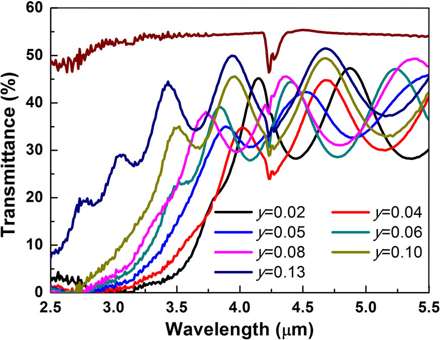
The measured spectral transmittance curves of thin films in the spectral range from 2.5 to 5.5 μm are demonstrated in Fig. 1. A spectrum of the silicon substrate is also presented in order to make a comparison. It can be clearly found that the absorption edges of thin films of can be tuned toward short wavelengths with the increase of the Ge concentration in films.
Figure 1.Measured spectral transmittance curves of thin films; a spectrum of the silicon substrate is also presented in order to make a comparison.
The optical constants (refractive index and extinction coefficient ) of thin films can be obtained by fitting the measured spectral transmittance curves using a Lorentz oscillator as a dispersion model. More details about the derivation of optical constants can be found in our previous studies[7,12].
It can be revealed in our investigation that a maximum refractive index and a minimum extinction coefficient exist simultaneously for thin films with a Ge concentration of 0.10, which were evaporated from the starting materials with a Ge concentration of 0.18. Therefore, the optimized optical properties can be obtained for the layer of by evaporating from the starting materials with a Ge concentration of 0.18 under a substrate temperature of 150°C, although the position of the fundamental absorption edge can still be shifted toward shorter wavelengths by evaporating from the starting materials with a Ge concentration of 0.25.
The optical constants of thin films evaporated from the starting materials with a Ge concentration of 0.18 are presented in Fig. 2. It was shown that the refractive index is greater than 5.0 in the spectral range from 2.5 to 5.5 μm. In particular, the extinction coefficient had the lowest value of 0.004 at 4.4 μm, which is comparable to the lowest value of the extinction coefficient obtainable for PbTe thin films.
Figure 2.Optical constants of thin films evaporated from the starting materials with a Ge concentration of 0.18.
A summary of the measured spectral transmittance curves in the spectral range from 0.2 to 8.5 μm is presented in Fig. 3 for the sapphire wafer, silicon wafer, Ge wafer, and thin films evaporated from the starting materials with a Ge concentration of 0.18, and PbTe thin films, respectively. The thicknesses of the wafers were 0.8 mm, while those of the thin films were 2 μm. The substrate temperature at which the thin films were deposited was 150°C. It is obvious that using as a high-index layer material, together with the sapphire wafer as the substrates, will assist in the blocking of bandpass filters in the spectral range of the mid-wavelength infrared.
Figure 3.Summary of measured spectral transmittance curves for the sapphire wafer, silicon wafer, Ge wafer, thin films, and PbTe thin films, respectively.
In order to demonstrate an improvement to the bandwidth of a thin-film bandpass filter using as a high-index material substituting for Ge, a simple 8-layer double cavity filter with a central wavelength of 4 μm was designed. In order to make a comparison, an equivalent thin-film narrow bandpass filter was also fabricated using Ge as the high-index material under completely identical conditions. Deposition was carried out on the sapphire substrates without rear-surface antireflection, as follows, where and represent, respectively, quarter-wave layers of and (or Ge). The layers of were evaporated from the starting materials with a Ge concentration of 0.18 using a molybdenum boat; meanwhile, the layers of and Ge were evaporated using electron beam heating. The substrate temperature was kept at 150°C.
The spectral transmittance curves for both filters were measured at room temperature. The measurements were reproducible, and no indication of hysteresis effect was observed. The results are presented in Fig. 4. The transmittances were plotted using logarithmic scales, which is particularly well suited whenever accurate information about the low transmission region is to be conveyed. It is demonstrated clearly that the filters fabricated using as high-index materials (black) have a narrower bandwidth than those fabricated using Ge as high-index materials (red). A value of 160 nm was obtained for the half-width of the filters fabricated using , whereas a value of 390 nm was obtained for those fabricated using Ge. Furthermore, the filters using have a superior rejection ratio to those using Ge.
Figure 4.Transmission spectrum of the narrowband filter fabricated using as a high-index material (black), compared with that using Ge as a high-index material (red).
In order to validate the integrity of the filters fabricated using as a high-index layer material, standard adhesion tests are performed to demonstrate the absence of a vulnerability to stress failures. In the test, a specified pressure-sensitive adhesive tape is pressed onto the surface of the filters and then peeled off again. The test procedure specifies that no coating material is removed; hence, the filters survived in the test, as shown in Fig. 5.
Figure 5.Standard adhesion tests are performed on the filters using as a high-index layer material.
In conclusion, is established as a potential candidate for high-index coating materials used in the mid-wavelength infrared narrow bandpass filters, in substituting for the convenient high-index material Ge.
References
[1] M. A. Macleod. Thin-Film Optical Filters(2010).
Ping Xie, Bin Li, Suying Zhang, Dingquan Liu, "Using lead germanium telluride as a high-index coating material in the mid-wavelength infrared narrow bandpass filters," Chin. Opt. Lett. 13, 123101 (2015)