• Photonics Research
  • Vol. 12, Issue 3, 465 (2024)
Zhicheng Jin, Jiageng Chen*, Yanming Chang, Qingwen Liu, and Zuyuan He
Author Affiliations
  • State Key Laboratory of Advanced Optical Communication System and Networks, Department of Electronic Engineering, Shanghai Jiao Tong University, Shanghai 200240, China
  • show less
    DOI: 10.1364/PRJ.512298 Cite this Article Set citation alerts
    Zhicheng Jin, Jiageng Chen, Yanming Chang, Qingwen Liu, Zuyuan He. Silicon photonic integrated interrogator for fiber-optic distributed acoustic sensing[J]. Photonics Research, 2024, 12(3): 465 Copy Citation Text show less

    Abstract

    Distributed acoustic sensing (DAS) technology has been a promising tool in various applications. Currently, the large size and relatively high cost of DAS equipment composed of discrete devices restrict its further popularization to some degree, and the photonic integration technology offers a potential solution. In this paper, we demonstrate an integrated interrogator for DAS on the silicon-on-insulator (SOI) platform. The design of the chip revolves around a Mach–Zehnder modulator (MZM) transmitter and a dual-quadrature and dual-polarization coherent receiver. The integrated interrogator supports multiple DAS schemes, including the time-gated digital optical frequency domain reflectometry (TGD-OFDR), which is adopted for system performance evaluation. 59 pε/Hz strain resolution in 12.1 km sensing fiber with 1.14 m spatial resolution (SR) is realized. Besides, along 49.0 km sensing fiber, 81 pε/Hz strain resolution with 3.78 m SR is achieved. The results show that the integrated interrogator has comparable performance to the discrete DAS system. To the best of our knowledge, this is the first dedicated on-chip DAS interrogator, which validates the effectiveness of the blend of photonics integration and DAS technology.

    1. INTRODUCTION

    Distributed acoustic sensing (DAS) is a fiber optic sensing technology that enables the measurement of dynamic strain signals along fiber optic cables with high sensitivity [1,2]. It utilizes the phase of Rayleigh backscattering (RBS) light for sensing and relies on time-of-flight for locating. The DAS system consists of a sensing fiber, an interrogator, and a data processing unit. Due to the advantages of high robustness against harsh environments, long-distance and high-density sensing capabilities, and high-fidelity information acquisition, DAS has been positioned as a powerful tool in diverse research and industry applications, such as geophysics observation [3], infrastructure monitoring [4], vehicle tracking [5], and border security systems [6]. Currently, DAS instruments usually rely on discrete optical and electronic devices, leading to bulky and expensive interrogators, which may hinder the widespread adoption of this technology. In applications such as aeronautics or space equipment, strict size and weight restrictions make traditional bulky DAS systems unsuitable. And in fields like the Internet of Things (IoT), consumer electronics, and many other industrial applications, the relatively high-cost DAS instruments have not been a very affordable solution yet.

    Photonic integration technology has emerged as a compelling solution for cost reduction and size minimization in electro-optic systems [79]. Over the past few decades, this technology has witnessed significant advances in the field of optical communication [10,11]. Besides, photonic integration technology can also facilitate the integration of various sensing systems. Notable examples include the on-chip spectrometer [12], integrated optical coherent tomography [13], integrated optical gyroscope [14], integrated fiber Bragg grating (FBG) interrogator [15], and on-chip biochemical sensor [16]. In terms of fiber optic sensing, photonic integration technology is employed to miniaturize the interrogator, which comprises a transmitter and a receiver. The current research on integrated interrogators for fiber optic sensing mainly focuses on FBG sensors [15,17,18], utilized for single-point or quasi-distributed sensing. On the other hand, for distributed optic-fiber sensing, Onbasli presented a design of an integrated non-coherent optical time domain reflectometry (OTDR) but has not completed tapeout [19], while Shishkin et al. made a preliminary attempt at optical frequency domain reflectometry (OFDR) integration [20]. Nonetheless, a dedicated photonic integrated circuit (PIC) for the DAS interrogator has yet to be realized.

    In this work, we report the first demonstration of an integrated DAS interrogator. The interrogator is based on the silicon-on-insulator (SOI) platform [21,22], which is known for its high index contrast enabling a high level of integration. In addition, the SOI platform is CMOS-compatible to meet low-cost requirements. The integrated interrogator comprises a Mach–Zehnder modulator (MZM) transmitter and a dual-quadrature and dual-polarization coherent receiver, which share a common external light source. The setup also incorporates auxiliary optics, including a polarization controller (PC) and an adjustable beam splitter (BS). Such an integrated interrogator is compatible with major DAS schemes, among which the time-gated digital optical frequency domain reflectometry (TGD-OFDR) scheme is chosen for the DAS performance evaluation. For a 12.1 km sensing fiber, the DAS system based on the integrated interrogator realizes a strain resolution of 59  /Hz under the spatial resolution (SR) of 1.14 m. And in another test using a longer 49.0 km sensing fiber, a strain resolution of 81  /Hz with 3.78 m SR is achieved.

    2. DESIGN OF THE INTEGRATED DAS INTERROGATOR

    A. Design Considerations

    Much research on DAS has been proposed based on various system configurations, from which some consensus on system architecture and design principles can be summarized. A DAS interrogator mainly includes a transmitter and a receiver. The transmitter generates a sequence of light pulses to interrogate the sensing fiber. A narrow linewidth continuous-wave (CW) laser is usually used as the light source, which cooperates with a modulator inside the transmitter. The receiver can share the CW laser as the local oscillator (LO) to implement the coherent heterodyne detection, which is a preferable and mainstream approach in DAS. Such architecture is the basis of the integrated DAS interrogator design.

    The modulator plays a key role in the interrogator. It is known that the acousto-optic modulator (AOM) is a conventional option in DAS systems [23], primarily attributed to its inherent frequency shifting capability, high extinction ratio, and low insertion loss (IL). Despite these benefits, the integrated AOM based on the SOI platform is still immature [24,25]. In another aspect, electro-optical modulators (EOMs) are also compatible with DAS [26], providing wider modulation bandwidth to achieve higher system performance [27]. In addition, the silicon photonics EOM is fully developed [2830], offering the feasibility to implement an integrated DAS interrogator. As for the selection between the micro-ring resonator (MRR) and the Mach–Zehnder interferometer (MZI), MRR-based modulators offer the advantage of a smaller footprint but are plagued by nonlinearity and limited thermal stability [31]. On the other hand, MZI-based EOMs have meticulous parameter balancing [21], making them a more suitable choice. There have been reports of DAS schemes using either MZMs (or called intensity modulators) or dual-parallel Mach–Zehnder modulators (DP-MZMs, often called QPSK or I/Q modulators) [26,32]. MZMs have sufficient performance and are relatively simple in signaling, while DP-MZMs support a wider range of modulation formats but require complex drive signals and configuration [33]. So, we select the MZM to implement the integrated DAS interrogator in this work.

    The coherent receiver with balanced detection is apparently more suitable for DAS whose measurand is the optical phase, in comparison with the direct detection scheme. The advantages include compatibility with heterodyne detection, common-mode interference suppression, and thermal noise reduction. In addition, the orthogonal phase diversity receiving scheme (called I/Q detection) provides a complex heterodyne signal whose positive/negative frequency components are separated. This enables a comprehensive phase demodulation, especially for signals not analytical for which Hilbert transform will no longer be valid, for example, the intensity-modulated double-sideband signal generated by the MZM. In order to achieve a satisfactory performance under a long measurement range, the polarization diversity configuration is necessary to compensate for the polarization fading effect of the RBS [34]. Furthermore, key features, such as the operating point of the MZM, the optical path difference for phase diversity receiving, and the power of LO, should be kept adjustable for the sake of robustness.

    The PIC design in this work is based on the above considerations. The DP-MZM-based DAS interrogator is also a reasonable alternative, and here we briefly discuss the PIC design of it. The use of DP-MZM in a DAS system is usually for a more complex or advanced modulation scheme. Since I/Q receivers are competent for any modulation formats by DP-MZM transmitters, a DP-MZM-based DAS PIC can be implemented by replacing the MZM with DP-MZM only and keeping all the others of the PIC in this work unchanged. One exception is that the DP-MZM is operating in single-sideband modulation mode. In such a condition, the I/Q receiving units can alternatively be simplified into bare balanced receivers, saving half of the channels in the post-stage analog and digitizer circuits. And associated controls should be taken to guarantee the proper bias points of the DP-MZM.

    B. Interrogator Chip

    An MZM-based integrated DAS interrogator is designed and implemented based on the aforementioned considerations. Figure 1(a) shows the microscope image of the PIC. It is fabricated on a standard 220 nm SOI platform with 3 μm upper oxide cladding and 3 μm buried oxide (BOX) through Advanced Micro Foundry’s (AMF) multi-project wafer (MPW) service [21]. The footprint of the whole chip is 5.9  mm×2.8  mm, while the functional area is 4.4  mm×2.8  mm. Figure 1(b) illustrates the schematic of the integrated DAS interrogator. The integrated DAS interrogator consists of a transmitter based on the MZM, a dual-quadrature and dual-polarization coherent receiver, and auxiliary integrated optics. The receiver comprises a polarization beam rotator splitter (PBRS), a 1×2 multimode interferometer (MMI), two 90° hybrids, and four balanced photodetectors (BPDs). Auxiliary integrated optics includes a PC and a BS. The interrogator also incorporates three suspended edge couplers [35], labeled “L”, “T”, and “R”, as input for the light source, output for modulated laser pulses, and input for backscattering light, respectively. All the on-chip elements are interconnected by passive strip waveguides with a width of 500 nm.

    (a) Microscope image of the photonic integrated circuit (PIC). (b) Schematic of the PIC. EC, edge coupler; PC, polarization controller; BS, beam splitter; MZM, Mach–Zehnder modulator; PBRS, polarization beam rotator splitter; MMI, multimode interferometer; BPD, balanced photodetector; LSI, low-speed electrical interface; HSI, high-speed electrical interface. “L”, “T”, and “R” denote the three edge couplers, serving as the input for the light source, the output for modulated laser pulses, and the input for RBS light, respectively. The arrangement of the elements and waveguides in the sketch is consistent with the chip in practice except for the electrical wires, while the aspect ratio is adjusted for a better view. (c)–(f) Magnified micrographs of the PC, MZM, 90° hybrid, and BPD.

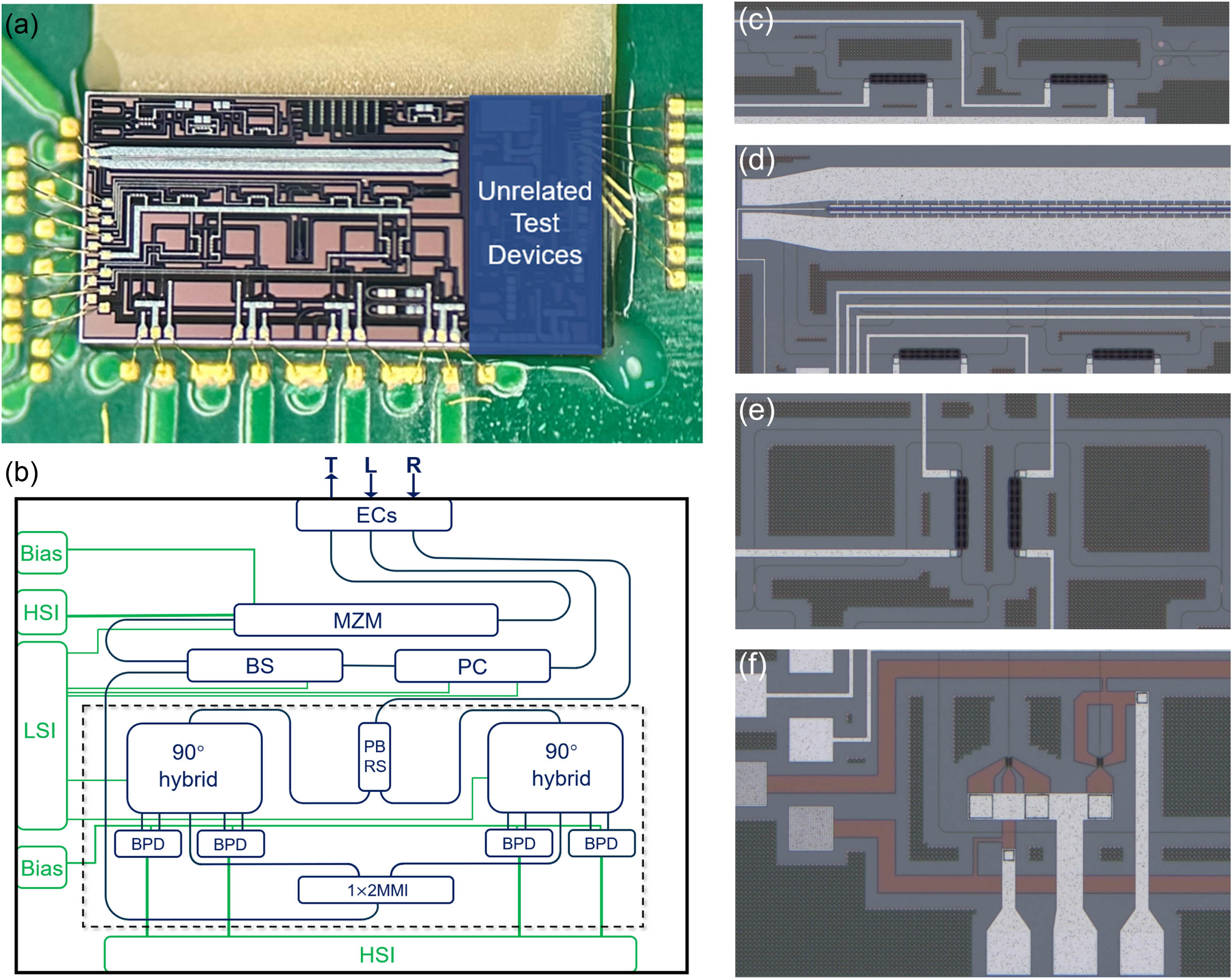
    Figure 1.(a) Microscope image of the photonic integrated circuit (PIC). (b) Schematic of the PIC. EC, edge coupler; PC, polarization controller; BS, beam splitter; MZM, Mach–Zehnder modulator; PBRS, polarization beam rotator splitter; MMI, multimode interferometer; BPD, balanced photodetector; LSI, low-speed electrical interface; HSI, high-speed electrical interface. “L”, “T”, and “R” denote the three edge couplers, serving as the input for the light source, the output for modulated laser pulses, and the input for RBS light, respectively. The arrangement of the elements and waveguides in the sketch is consistent with the chip in practice except for the electrical wires, while the aspect ratio is adjusted for a better view. (c)–(f) Magnified micrographs of the PC, MZM, 90° hybrid, and BPD.

    A narrow linewidth CW laser enters the PIC from the “L” port and first passes the PC. When appropriately adjusted, the PC effectively converts input lights of any polarization state into the pure TE mode. The PC consists of two cascaded MZI structures whose phase difference of two arms can be adjusted by a thermo-optical phase shifter (TPS) [36], and a following polarization beam splitter (PBS) is used to strip out the TM mode light thoroughly. The magnified micrograph of the PC is shown in Fig. 1(c). The CW laser is then split by the BS into two beams: one is directed toward the MZM, while the other serves as the LO for the coherent receiver. Since the optimal power of the LO depends on multiple factors, such as the power of the light source, saturation power of the photodetector (PD), strength of the RBS light, and other in-situ configurations, the splitting ratio is adjustable to accommodate these considerations. The MZI-based BS utilizes TPS for tuning, providing a satisfactory dynamic range that meets the system’s requirements.

    Figure 1(d) illustrates the MZM designed utilizing the provided design cells from the process design kit (PDK) of AMF [29]. Leveraging the plasma dispersion effect, the MZM exhibits a high enough bandwidth [21] to fulfill the requirements of DAS systems, which typically operate below 1 GHz. To achieve a balance, a compromise length of 3.8 mm is selected for the PN junction, resulting in an IL of approximately 5 dB and a half-wave voltage (Vπ) of around 6 V. This length also ensures compliance with the size restriction of the chip. A TPS cascaded with the PN junction is employed to control the operating point of the MZM. The operating point should be kept at the null point for pulse generation. The light modulated by the MZM is then emitted from the interrogator through the “T” port.

    The RBS light from the sensing fiber enters the PIC from the “R” port. To accomplish the polarization diversity coherent detection, the PBRS performs polarization separation of RBS light, and the TM mode RBS light is converted into TE mode. The 1×2 MMI equally splits the LO mentioned before. The RBS and LO then enter two identical orthogonal balanced receiving units, each containing one 90° hybrid and two BPDs. The magnified micrograph of the hybrid is depicted in Fig. 1(e). It is worth noting that, in DAS systems, coherent receivers require a strict phase orthogonality of the hybrids. Therefore, the scheme including TPS [37] instead of passive 2×4 MMI or 4×4 MMI [38,39] is chosen to implement the hybrid, allowing precise adjustment of the phase shift around 90°. The hybrid mixes the RBS light and the LO, and all the outputs of the hybrids are then fed into four BPDs. The transmission waveguides between hybrids and BPDs have the same length to ensure identical time delays. The structure of the BPD is presented in Fig. 1(f), where two germanium PDs are connected by metal layers to achieve balanced detection. The BPDs output I/Q heterodyne signals, for RBS light in TE and TM modes, respectively.

    The PIC is co-packed with a fiber array and a printed circuit board assembly (PCBA), as shown in Fig. 2. The PIC and the fiber array are fixed together through a simple packaging using ultraviolet curing, where the matching oil is required and should be carefully selected to minimize the coupling loss [35]. The fiber array provides connections for external optical devices. The PCBA contains electric connectors for bias, tuning, and modulation signals for the PIC, as well as four identical transimpedance amplifier (TIA) circuits. The overall footprint of the PCBA is 112  mm×107  mm. The TIAs collaborate with the on-chip PD pairs to form complete BPDs with a cutoff frequency of 1.5 GHz and an overall conversion coefficient of 13.5 kV/W. Such parameters are more proper for DAS compared with typical TIAs for communication purposes, whose bandwidth is redundant and often contains functional units, such as the automatic gain control circuit, that are not required for DAS. To achieve the desired performance, the TIAs are carefully designed. The output signals of the TIAs are directed from the RF ports to the external device for signal acquisition and processing.

    Image of the packaged PIC for the DAS interrogator.

    Figure 2.Image of the packaged PIC for the DAS interrogator.

    C. DAS System Configuration

    The integrated interrogator supports a variety of DAS modulation/demodulation schemes. We select the TGD-OFDR scheme to implement the DAS system [26]. By employing linear frequency modulated (LFM) pulses and match filtering demodulation technique, TGD-OFDR can achieve higher performance compared with classical DAS schemes such as the φ-OTDR. The system configuration is depicted in Fig. 3. A narrow linewidth laser (NKT E-15) serves as the light source to provide 1550 nm CW light via the “L” port. An erbium-doped fiber amplifier (EDFA) boosts the probe light from the “T” port of the PIC, and an optical circulator guides the boosted probe light into the sensing fiber and guides the RBS light back to the “R” port. An arbitrary waveform generator (AWG, Keysight M8195A) generates LFM pulses. After passing an RF amplifier, the LFM pulses drive the modulator inside the PIC. Low-speed control and bias signals for the interrogator chip are provided by a multi-channel signal source. Data acquisition cards (DAQs, NI PXIe-5185×2) and a computer acquire and process the output signals from the BPDs. The AWG and DAQs are synchronized in triggering and clocking for proper cooperation. The sensing fiber is G.652.D standard single-mode fiber, and a piezoelectric transducer (PZT) is attached at the end of the sensing fiber to apply dynamic strain signals for testing.

    Schematic of the DAS system based on TGD-OFDR. PIC, photonic integrated circuit; TIA, transimpedance amplifier; EDFA, erbium-doped fiber amplifier; PZT, piezoelectric transducer; SG, signal generator; LFM, linear frequency modulator; AWG, arbitrary waveform generator; DAQ, data acquisition card; DSP, digital signal processing.

    Figure 3.Schematic of the DAS system based on TGD-OFDR. PIC, photonic integrated circuit; TIA, transimpedance amplifier; EDFA, erbium-doped fiber amplifier; PZT, piezoelectric transducer; SG, signal generator; LFM, linear frequency modulator; AWG, arbitrary waveform generator; DAQ, data acquisition card; DSP, digital signal processing.

    The modulation signal can be expressed as VRF(t)={V0cos(2πf0t+πκt2),t[0,τp]0,t(τp,Tp],where V0=3  V is the amplitude of the RF signal corresponding to α=V0/Vπ=0.5, f0=100  MHz is the initial frequency, κ=50  MHz/μs is the frequency sweep rate, and τp=20  μs is the pulse duration. Such specification corresponds to LFM pulses from 100 MHz to 1.1 GHz during 20 μs. Tp denotes the repetition period of the LFM pulses, which is relative to the length of the sensing fiber. Additionally, a DC signal should be used to set the operating point of the modulator to the null point. The outputs of four BPDs can be denoted as VI,TE, VQ,TE, VI,TM, VQ,TM, respectively. During data processing, the four signals are grouped into two complex signals VTE and VTM, which can be expressed as {VTE(t)=VI,TE(t)+jVQ,TE(t)VTM(t)=VI,TM(t)+jVQ,TM(t).These complex signals are used in the demodulation algorithm of TGD-OFDR. Optimizations encompass the rotated-vector-sum method and the moving averaging method, and other relevant techniques as described in Refs. [26,40,41] are also employed.

    3. EXPERIMENT RESULTS

    A. Basic Tests of the Interrogator Chip

    Several preliminary tests are performed before the system-level experiment. The first test measures the IL of the path between the “L” port and the “T” port. During the measurement, the MZM is set at its peak point with 0.5  V bias, the BS is adjusted to direct all light into the MZM, and the control voltages of the PC are appropriately configured. The IL is measured to be 10.5  dB in total, including 5  dB IL contributed by the MZM, 3  dB coupling loss from two packaged edge couplers of the “L” port and “T” port, and the rest from the PC, the BS, and the waveguides. Such an IL is 5  dB larger than that of a typical discrete interrogator in the lab (modulator model: Optilab IM-1550-20). However, the post-stage optical amplifier, which is necessary for either discrete or integrated DAS integrators, can compensate for it well. Besides, the extinction ratio of the MZM is measured to be 25  dB, by switching the MZM from the peak point to the null point. Such extinction ratio is sufficient for the TGD-OFDR, due to the employment of pulse compression technique, which relaxes the requirement on extinction ratio.

    Tests on the receiver follow the configuration depicted in Fig. 4(a). The MZM is set to the peak point while no RF signal is applied. An external AOM introduces a perfect 80 MHz single frequency shift into the laser, and an external PC adjusts the laser entering the “R” port to contain TE and TM mode components in approximately equal power. For an ideal receiver, the VTE and VTM in Eq. (2) are single-frequency complex signals. Otherwise, other frequency components will appear in VTE or VTM, which will distort DAS demodulation. So the sideband suppression ratio (SSR) can be used to evaluate the quality of the receiver. Figures 4(b) and 4(c) show the spectra of measured VTE and VTM, respectively. The corresponding SSRs are 41.9 dB and 33.8 dB. For comparison, we test the SSRs of a commercial discrete 90° optical hybrid with the polarization diversity feature (Optoplex HB-COGFAS002), which are 25 dB and 30 dB for two polarizations, respectively. During a long-term test, the SSRs of VTE and VTM remain above 41 dB and 32 dB, respectively, as shown in Fig. 4(d). The difference between the two orthogonal receiving units can be attributed to potential fabrication process inconsistencies and limited tuning resolution of the configuration voltages, as suggested by the authors. The slight long-term drift may be partially attributed to the fluctuations of the multi-channel signal source. In subsequent DAS performance evaluations, on-chip hybrids use the same configuration voltages as the aforementioned test.

    Experiment setup and results for tests on the receiver. (a) Schematic diagram of the test system. (b) Spectrum of VTE with 80 MHz frequency shift. (c) Spectrum of VTM with 80 MHz frequency shift. (d) Sideband suppression ratio (SSR) of VTE (blue) and VTM (red) over 2 h. Values at the starting time correspond to results in (b) and (c), respectively.

    Figure 4.Experiment setup and results for tests on the receiver. (a) Schematic diagram of the test system. (b) Spectrum of VTE with 80 MHz frequency shift. (c) Spectrum of VTM with 80 MHz frequency shift. (d) Sideband suppression ratio (SSR) of VTE (blue) and VTM (red) over 2 h. Values at the starting time correspond to results in (b) and (c), respectively.

    B. DAS Performance

    The experiment setup is depicted in Fig. 3. The first DAS experiment takes 12.1 km of sensing fiber. PZT at the end of sensing fiber is driven by a 100 Hz sinusoidal signal and coiled with approximately 2 m of fiber. The repetition rate of the LFM pulses is 5 kHz, the gauge length is 0.819 m, and 300 temporally adjacent traces are recorded during the measurement. The configuration is similar to the previous work by the authors [26] for comparison. Figure 5(a) shows the demodulated RBS intensity traces after fading suppression, from which it can be seen that the overall signal-to-noise ratio (SNR) along the entire fiber is above 25 dB. The distance-time distribution of the differential phases is depicted in Fig. 5(b), and the applied vibration at the end of the sensing fiber can be discerned as shown in the inset figure. Figure 5(c) gives the calculated standard deviation (SD) of the differential phases along the fiber. The SR can be obtained from the inset figure in Fig. 5(c), which is 1.14 m, based on the definition of the average value of 10% to 90% rising edge and falling edge. The phase waveform at a distance of 12,104.18 m can be extracted from Fig. 5(b) and is presented in Fig. 5(d), and the corresponding power spectral density (PSD) is shown in Fig. 5(e). The peak at 100 Hz in the PSD curve consists well with the applied vibration. By averaging the PSD curve (in the unit of rad2/Hz) excluding a narrow range near the peak, the self-noise level can be calculated to be 1.91×10⁷  rad2/Hz, corresponding to a strain resolution of 59  /Hz under the 0.819 m gauge length [41]. Such performance is comparable to the discrete TGD-OFDR DAS system in Ref. [26].

    Demodulation results for the 12.1 km sensing fiber. (a) Normalized intensity traces with polarization fading suppressed (green) and with fading (red and blue). (b) Distance–time distribution of the differential phases along the fiber, with a vibration applied at around 12.1 km. (c) Phase standard deviation (SD) trace along the fiber with a spatial resolution (SR) of 1.14 m. (d) Waveform of the 100 Hz vibration from 10 ms to 40 ms. (e) Power spectral density (PSD) of the measured variation. The self-noise level is shown as the red dashed line.

    Figure 5.Demodulation results for the 12.1 km sensing fiber. (a) Normalized intensity traces with polarization fading suppressed (green) and with fading (red and blue). (b) Distance–time distribution of the differential phases along the fiber, with a vibration applied at around 12.1 km. (c) Phase standard deviation (SD) trace along the fiber with a spatial resolution (SR) of 1.14 m. (d) Waveform of the 100 Hz vibration from 10 ms to 40 ms. (e) Power spectral density (PSD) of the measured variation. The self-noise level is shown as the red dashed line.

    The second experiment takes 49.0 km sensing fiber and presets parameters corresponding to an SR of 4  m, which is a typical configuration for commercial long-range DAS systems. 10 m of fiber is wrapped around the PZT (100 Hz sinusoidal strain applied), the repetition rate of LFM pulses is 1.5 kHz, and 120 traces adjacent in time are captured during the measurement. The experimental results are shown in Fig. 6. The demodulated RBS intensity traces are plotted in Fig. 6(a), showing an SNR above 15 dB at the end of the sensing fiber after polarization and interference fading suppression. Figure 6(b) shows the distance-time distribution of the differential phases, and the vibration signal can be clearly discerned without any presence of erroneous phases. The SR can be obtained from the inset graph in Fig. 6(c), which is 3.78 m. Figure 6(d) plots the measured waveform at 49,022.32 m and the corresponding PSD is depicted in Fig. 6(e). The self-noise level at the end of the fiber is calculated to be 8.59×10⁶  rad2/Hz, corresponding to a strain resolution of 81  /Hz under the 4.01 m gauge length, which meets the quality of long-range commercial DAS systems.

    Demodulation results for the 49.0 km sensing fiber. (a) Normalized intensity traces with polarization fading suppressed (green) and with fading (red and blue). (b) Distance–time distribution of the differential phases along the fiber, with a vibration applied at around 49.0 km. (c) Phase SD trace along the fiber with 3.78 m SR. (d) Waveform of the 100 Hz vibration from 40 ms to 70 ms. (e) PSD of the measured variation.

    Figure 6.Demodulation results for the 49.0 km sensing fiber. (a) Normalized intensity traces with polarization fading suppressed (green) and with fading (red and blue). (b) Distance–time distribution of the differential phases along the fiber, with a vibration applied at around 49.0 km. (c) Phase SD trace along the fiber with 3.78 m SR. (d) Waveform of the 100 Hz vibration from 40 ms to 70 ms. (e) PSD of the measured variation.

    In order to investigate the DAS performance under the rather low SNR condition, we further extend the length of the sensing fiber to 74.1 km. The repetition rate of pulses is 1.2 kHz, and the gauge length keeps 4.01 m. A total of 96 adjacent traces are recorded in one measurement. Figure 7(a) shows the calculated strain resolution along the sensing fiber. It can be observed that beyond 50 km the strain resolution will evidently worsen as the distance increases. This is consistent with the experience in DAS systems based on discrete devices. Taking an empirical threshold of acceptable strain resolution of 150  /Hz, the limiting measurement range can reach 70  km. Figure 7(b) shows the demodulated waveform of the 100 Hz sinusoidal vibration at the end of the 74.1 km sensing fiber, and the corresponding strain resolution is 0.3  /Hz.

    Demodulation results for the 74.1 km sensing fiber. (a) Strain resolution distribution along the sensing fiber. (b) Waveform of the 100 Hz vibration from 10 ms to 50 ms.

    Figure 7.Demodulation results for the 74.1 km sensing fiber. (a) Strain resolution distribution along the sensing fiber. (b) Waveform of the 100 Hz vibration from 10 ms to 50 ms.

    The above results demonstrate the performance of the MZM-based integrated DAS interrogator. It is known that the cost of a DAS interrogator mainly includes the light source, the optical circuit, and the signal processing electronics. The proposed PIC shows great potential to reduce the cost of the optical circuit composed of commercial discrete devices, which is worth several thousand dollars in the current stage. By further developing it into a fully integrated DAS interrogator, not only would the integration level improve, but the cost could also be significantly reduced. At the current stage of the work, the light source, the optical amplifier, and the optical circulator are not integrated yet, due to the well-known obstacle that silicon does not have a direct bandgap nor is it nonreciprocal. Nonetheless, there are ongoing techniques such as hybrid integration, heterogeneous integration, and monolithic integration offering promising solutions [42,43]. Hybrid-integrated tunable external cavity lasers [44] show potential in meeting the linewidth requirements of DAS systems. The state-of-the-art heterogeneously integrated III-V-on-silicon amplifiers proposed by Van Gasse et al. can provide a small signal gain of 27 dB and a saturation power of 17.24 dBm [45]. The silicon-integrated magneto-optical nonreciprocal devices have exhibited high isolation ratios up to 30  dB and low IL down to 2  dB [46]. In addition to utilizing other materials, there are alternative approaches that offer integration possibilities. The chip-scale version of the EDFA is realized using a spiral of erbium-doped silicon nitride waveguide in a compact footprint of 1.2  mm×3.6  mm with a performance comparable to that of commercially available EDFA modules [47], and nonlinear optical effects of waveguides can be leveraged to implement nonreciprocal devices that are CMOS-compatible [48]. Considering these advancements, there is a promising prospect to achieve a fully integrated DAS interrogator.

    The PIC shows expectable long-term stability during the laboratory test, which is mainly because high-power devices leading to severe heat dissipation or thermal gradient, or highly thermal-sensitive structures are not included, in the authors’ opinion. In harsh environments, the feedback tuning of photonic devices is an effective approach to compensate for the impact of environmental disturbances [49]. The dithering method can maintain the operating point stability of MZM [50], while various automatic polarization control algorithms have been proposed to realize integrated polarization stabilizers [51]. And I/Q imbalance solutions applied to discrete systems can provide ideas for on-chip hybrid stabilization [52,53]. Additionally, in terms of packaging, the introduction of a thermoelectric cooler (TEC) can enhance the temperature stability of the system. By further implementing the aforementioned approaches, the stability of the PIC can be improved.

    4. CONCLUSION

    We presented an integrated DAS interrogator based on the SOI platform, and to the best of our knowledge, it is the first realization of a dedicated PIC for DAS. This integrated DAS interrogator supports various DAS schemes, including the TGD-OFDR, which is taken for system performance evaluation. Strain resolution of 59  /Hz with 1.14 m SR along 12.1 km sensing fiber, and strain resolution of 81  /Hz with 3.78 m SR along 49.0 km fiber, are realized, respectively. The performance is comparable to the recently reported discrete DAS system and can meet commercial requirements, validating the feasibility and effectiveness of the blend of photonics integration and DAS technology.

    Acknowledgment

    Acknowledgment. The authors thank Advanced Micro Foundry (AMF) for offering multi-project wafer (MPW) service.

    References

    [1] B. G. Gorshkov, K. Yüksel, A. A. Fotiadi. Scientific applications of distributed acoustic sensing: state-of-the-art review and perspective. Sensors, 22, 1033(2022).

    [2] Z. He, Q. Liu. Optical fiber distributed acoustic sensors: a review. J. Lightwave Technol., 39, 3671-3686(2021).

    [3] M. R. Fernández-Ruiz, M. A. Soto, E. F. Williams. Distributed acoustic sensing for seismic activity monitoring. APL Photon., 5, 030901(2020).

    [4] E. G. Bakhoum, C. Zhang, M. H. Cheng. Real time measurement of airplane flutter via distributed acoustic sensing. Aerospace, 7, 125(2020).

    [5] M.-F. Huang, M. Salemi, Y. Chen. First field trial of distributed fiber optical sensing and high-speed communication over an operational telecom network. J. Lightwave Technol., 38, 75-81(2019).

    [6] S. A. Aslangul. Detecting tunnels for border security based on fiber optical distributed acoustic sensor data using dbscan. Sensornets, 78-84(2020).

    [7] T. Komljenovic, D. Huang, P. Pintus. Photonic integrated circuits using heterogeneous integration on silicon. Proc. IEEE, 106, 2246-2257(2018).

    [8] T. Sharma, J. Wang, B. K. Kaushik. Review of recent progress on silicon nitride-based photonic integrated circuits. IEEE Access, 8, 195436-195446(2020).

    [9] W. Shi, Y. Tian, A. Gervais. Scaling capacity of fiber-optic transmission systems via silicon photonics. Nanophotonics, 9, 4629-4663(2020).

    [10] S. Yamanaka, Y. Ikuma, T. Itoh. Silicon photonics coherent optical subassembly with eo and oe bandwidths of over 50 GHz. Optical Fiber Communication Conference, Th4A–4(2020).

    [11] S. Yamanaka, Y. Nasu. Silicon photonics coherent optical subassembly for high-data-rate signal transmissions. Optical Fiber Communication Conference, Th5F–2(2021).

    [12] A. Li, C. Yao, J. Xia. Advances in cost-effective integrated spectrometers. Light Sci. Appl., 11, 174(2022).

    [13] E. A. Rank, R. Sentosa, D. J. Harper. Toward optical coherence tomography on a chip: in vivo three-dimensional human retinal imaging using photonic integrated circuit-based arrayed waveguide gratings. Light Sci. Appl., 10, 6(2021).

    [14] Y.-H. Lai, M.-G. Suh, Y.-K. Lu. Earth rotation measured by a chip-scale ring laser gyroscope. Nat. Photonics, 14, 345-349(2020).

    [15] H. Li, Z. An, S. Zhang. Fully photonic integrated wearable optical interrogator. ACS Photon., 8, 3607-3618(2021).

    [16] Y. E. Marin, V. Toccafondo, P. Velha. Silicon photonic biochemical sensor on chip based on interferometry and phase-generated-carrier demodulation. IEEE J. Sel. Top. Quantum Electron., 25, 5200109(2018).

    [17] M. Słowikowski, A. Kaźmierczak, S. Stopiński. Photonic integrated interrogator for monitoring the patient condition during MRI diagnosis. Sensors, 21, 4238(2021).

    [18] J. Elaskar, F. Bontempi, P. Velha. Ultracompact microinterferometer-based fiber Bragg grating interrogator on a silicon chip. J. Lightwave Technol., 41, 4397-4404(2023).

    [19] M. C. Onbaşli. Photonic integrated circuit-assisted optical time-domain reflectometer system. Turkish J. Electr. Eng. Comput. Sci., 30, 579-591(2022).

    [20] V. Shishkin, K. Tanaka, H. Murayama. Proposal on miniaturization of distributed sensing system based on optical frequency domain reflectometry. Transdisciplinary Engineering for Complex Socio-technical Systems, 22-29(2019).

    [21] S. Y. Siew, B. Li, F. Gao. Review of silicon photonics technology and platform development. J. Lightwave Technol., 39, 4374-4389(2021).

    [22] A. Rahim, T. Spuesens, R. Baets. Open-access silicon photonics: current status and emerging initiatives. Proc. IEEE, 106, 2313-2330(2018).

    [23] Q. Liu, X. Fan, Z. He. Time-gated digital optical frequency domain reflectometry with 1.6-m spatial resolution over entire 110-km range. Opt. Express, 23, 25988-25995(2015).

    [24] J. Beller, L. Shao. Acousto-optic modulators integrated on-chip. Light Sci. Appl., 11, 240(2022).

    [25] E. A. Kittlaus, W. M. Jones, P. T. Rakich. Electrically driven acousto-optics and broadband non-reciprocity in silicon photonics. Nat. Photonics, 15, 43-52(2021).

    [26] D. Chen, Q. Liu, Z. He. High-fidelity distributed fiber-optic acoustic sensor with fading noise suppressed and sub-meter spatial resolution. Opt. Express, 26, 16138-16146(2018).

    [27] J. Jiang, Z. Wang. Continuous chirped-wave phase-sensitive optical time-domain reflectometry: principles and demonstrations. 19th International Conference on Optical Communications and Networks (ICOCN), 1-3(2021).

    [28] A. Rahim, A. Hermans, B. Wohlfeil. Taking silicon photonics modulators to a higher performance level: state-of-the-art and a review of new technologies. Adv. Photon., 3, 024003(2021).

    [29] D. Patel, S. Ghosh, M. Chagnon. Design, analysis, and transmission system performance of a 41 GHz silicon photonic modulator. Opt. Express, 23, 14263-14287(2015).

    [30] S. Saha, R. Roy, S. Pal. Performance analysis of an electrostatic doping assisted dual parallel Mach-Zehnder modulator. Advances in Smart Communication Technology and Information Processing: OPTRONIX 2020, 47-57(2021).

    [31] K. Padmaraju, J. Chan, L. Chen. Thermal stabilization of a microring modulator using feedback control. Opt. Express, 20, 27999-28008(2012).

    [32] Y. Wakisaka, D. Iida, H. Oshida. Fading suppression of ϕ-OTDR with the new signal processing methodology of complex vectors across time and frequency domains. J. Lightwave Technol., 39, 4279-4293(2021).

    [33] H. Chen, B. Zhang, L. Hu. Thermo-optic-based phase-shifter power dither for silicon IQ optical modulator bias-control technology. Opt. Express, 27, 21546-21564(2019).

    [34] M. Ren, P. Lu, L. Chen. Theoretical and experimental analysis of ϕ-OTDR based on polarization diversity detection. IEEE Photon. Technol. Lett., 28, 697-700(2015).

    [35] L. Jia, C. Li, T.-Y. Liow. Efficient suspended coupler with loss less than −1.4 dB between Si-photonic waveguide and cleaved single mode fiber. J. Lightwave Technol., 36, 239-244(2017).

    [36] M. Ma, K. Murray, M. Ye. Silicon photonic polarization receiver with automated stabilization for arbitrary input polarizations. CLEO: Science and Innovations, STu4G–8(2016).

    [37] S. Faralli, G. Meloni, F. Gambini. A compact silicon coherent receiver without waveguide crossing. IEEE Photon. J., 7, 7802806(2015).

    [38] W. Yang, M. Yin, Y. Li. Ultra-compact optical 90 hybrid based on a wedge-shaped 2 × 4 mmi coupler and a 2 × 2 MMI coupler in silicon-on-insulator. Opt. Express, 21, 28423-28431(2013).

    [39] K. Voigt, L. Zimmermann, G. Winzer. C-band optical 90° hybrids in silicon nanowaveguide technology. IEEE Photon. Technol. Lett., 23, 1769-1771(2011).

    [40] D. Chen, Q. Liu, Z. He. Phase-detection distributed fiber-optic vibration sensor without fading-noise based on time-gated digital OFDR. Opt. Express, 25, 8315-8325(2017).

    [41] D. Chen, Q. Liu, Z. He. Distributed fiber-optic acoustic sensor with sub-nano strain resolution based on time-gated digital OFDR. Asia Communications and Photonics Conference, S4A–2(2017).

    [42] P. Kaur, A. Boes, G. Ren. Hybrid and heterogeneous photonic integration. APL Photon., 6, 061102(2021).

    [43] S. Shekhar, W. Bogaerts, L. Chrostowski. Silicon photonics–roadmapping the next generation. arXiv(2023).

    [44] Y. Guo, X. Li, M. Jin. Hybrid integrated external cavity laser with a 172-nm tuning range. APL Photon., 7, 066101(2022).

    [45] K. Van Gasse, R. Wang, G. Roelkens. 27 db gain III–V-on-silicon semiconductor optical amplifier with >17  dBm output power. Opt. Express, 27, 293-302(2019).

    [46] W. Yan, Y. Yang, W. Yang. On-chip nonreciprocal photonic devices based on hybrid integration of magneto-optical garnet thin films on silicon. IEEE J. Sel. Top. Quantum Electron., 27, 6100515(2021).

    [47] Y. Liu, Z. Qiu, X. Ji. A photonic integrated circuit–based erbium-doped amplifier. Science, 376, 1309-1313(2022).

    [48] L. Fan, J. Wang, L. T. Varghese. An all-silicon passive optical diode. Science, 335, 447-450(2012).

    [49] M. Tan, K. Ye, D. Ming. Towards electronic-photonic-converged thermo-optic feedback tuning. J. Semicond., 42, 023104(2021).

    [50] H. Chen, B. Zhang, W. Ma. Study on auto bias control of a silicon optical modulator in a four-level pulse amplitude modulation format. Appl. Opt., 58, 3986-3994(2019).

    [51] M. Ma, H. Shoman, K. Tang. Automated control algorithms for silicon photonic polarization receiver. Opt. Express, 28, 1885-1896(2020).

    [52] Y. Fu, N. Xue, Z. Wang. Impact of I/Q amplitude imbalance on coherent ϕ-OTDR. J. Lightwave Technol., 36, 1069-1075(2018).

    [53] N. Xue, Y. Fu, C. Lu. Characterization and compensation of phase offset in ϕ-OTDR with heterodyne detection. J. Lightwave Technol., 36, 5481-5487(2018).

    Zhicheng Jin, Jiageng Chen, Yanming Chang, Qingwen Liu, Zuyuan He. Silicon photonic integrated interrogator for fiber-optic distributed acoustic sensing[J]. Photonics Research, 2024, 12(3): 465
    Download Citation