• Chinese Optics Letters
  • Vol. 19, Issue 10, 101302 (2021)
Xiaorui Li, Liangjun Lu*, Wei Gao, Xin Li, Jianping Chen, and Linjie Zhou
Author Affiliations
  • State Key Laboratory of Advanced Optical Communication Systems and Networks, Shanghai Institute for Advanced Communication and Data Science, Shanghai Key Laboratory of Navigation and Location Services, Department of Electronic Engineering, Shanghai Jiao Tong University, Shanghai 200240, China
  • show less
    DOI: 10.3788/COL202119.101302 Cite this Article Set citation alerts
    Xiaorui Li, Liangjun Lu, Wei Gao, Xin Li, Jianping Chen, Linjie Zhou. Silicon non-blocking 4 × 4 optical switch with automated polarization adjustment[J]. Chinese Optics Letters, 2021, 19(10): 101302 Copy Citation Text show less
    (a) Schematic structure of the polarization-insensitive 4 × 4 MZI switch chip. The inset shows the on-chip polarization controller and the control system. (b) Microscope image of the fabricated silicon 4 × 4 optical switch chip. (c) Photo of the packaged chip.
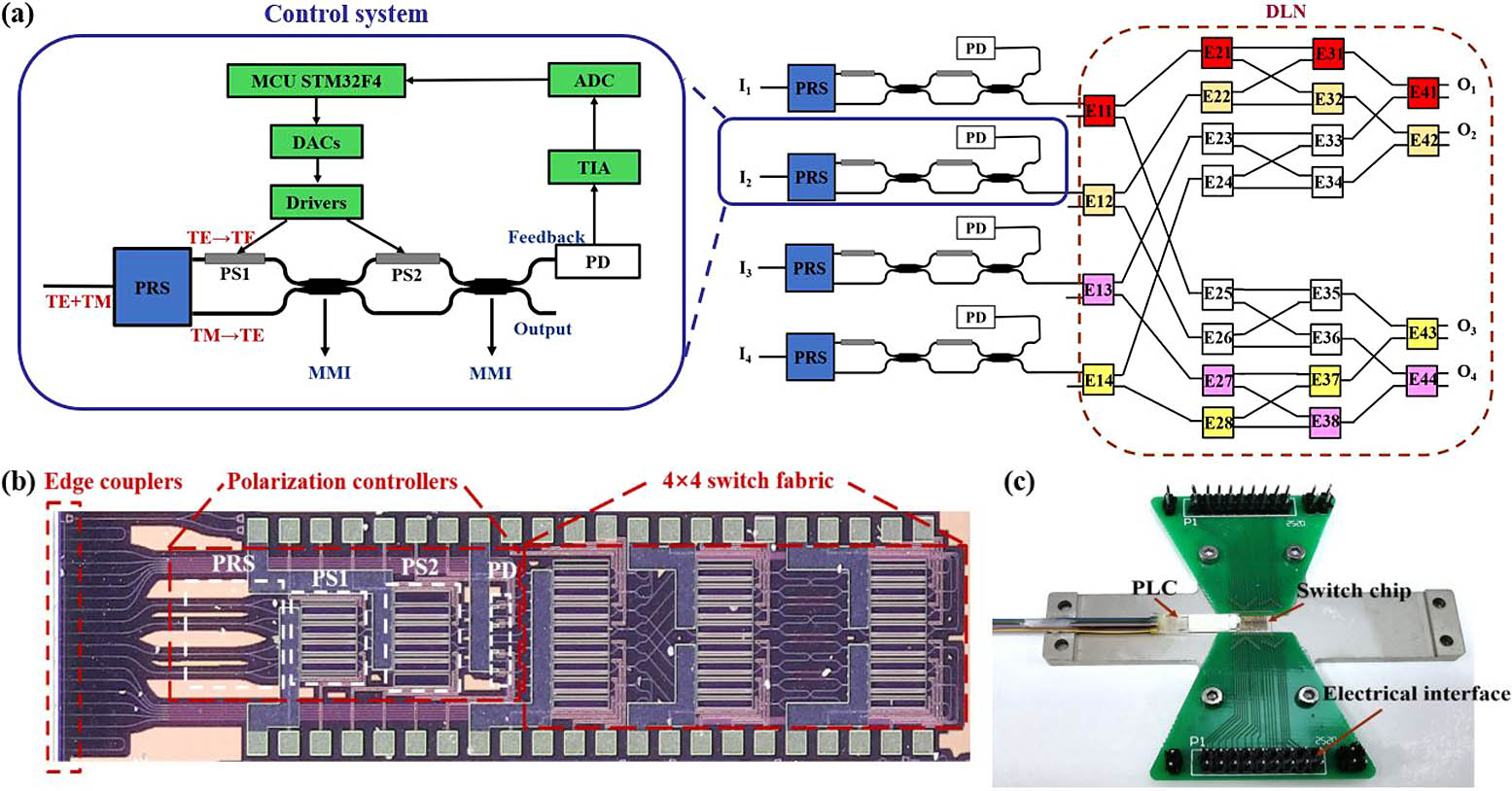
    Fig. 1. (a) Schematic structure of the polarization-insensitive 4 × 4 MZI switch chip. The inset shows the on-chip polarization controller and the control system. (b) Microscope image of the fabricated silicon 4 × 4 optical switch chip. (c) Photo of the packaged chip.
    Normalized feedback port power Pf as a function of Δφ1 and Δφ2 with different combinations of input polarizations: (a) TE 25%, TM 75%; (b) TE 50%, TM 50%; (c) TE 75%, TM 25%; and (d) TE 100%.
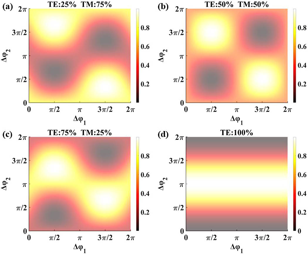
    Fig. 2. Normalized feedback port power Pf as a function of Δφ1 and Δφ2 with different combinations of input polarizations: (a) TE 25%, TM 75%; (b) TE 50%, TM 50%; (c) TE 75%, TM 25%; and (d) TE 100%.
    Flow chart of the polarization control algorithm.
    Fig. 3. Flow chart of the polarization control algorithm.
    (a), (b) Polarization tuning process for two random polarization states. (c), (d) Recorded TIA voltages with randomly changed input polarization when the algorithm is (c) turned off and (d) turned on.
    Fig. 4. (a), (b) Polarization tuning process for two random polarization states. (c), (d) Recorded TIA voltages with randomly changed input polarization when the algorithm is (c) turned off and (d) turned on.
    Measured transmission spectra of the I2−O2 path for different input polarization states after polarization adjustment.
    Fig. 5. Measured transmission spectra of the I2O2 path for different input polarization states after polarization adjustment.
    Measured transmission spectra of one switching state at (a) port O1, (b) port O2, (c) port O3, and (d) port O4.
    Fig. 6. Measured transmission spectra of one switching state at (a) port O1, (b) port O2, (c) port O3, and (d) port O4.
    Optical transmission measurement of a 32 Gbit/s OOK signal for various input polarization states: (a) eye diagrams and (b) BER as a function of received optical power.
    Fig. 7. Optical transmission measurement of a 32 Gbit/s OOK signal for various input polarization states: (a) eye diagrams and (b) BER as a function of received optical power.
    Xiaorui Li, Liangjun Lu, Wei Gao, Xin Li, Jianping Chen, Linjie Zhou. Silicon non-blocking 4 × 4 optical switch with automated polarization adjustment[J]. Chinese Optics Letters, 2021, 19(10): 101302
    Download Citation