• Chinese Optics Letters
  • Vol. 19, Issue 10, 101302 (2021)
Xiaorui Li, Liangjun Lu*, Wei Gao, Xin Li, Jianping Chen, and Linjie Zhou
Author Affiliations
  • State Key Laboratory of Advanced Optical Communication Systems and Networks, Shanghai Institute for Advanced Communication and Data Science, Shanghai Key Laboratory of Navigation and Location Services, Department of Electronic Engineering, Shanghai Jiao Tong University, Shanghai 200240, China
  • show less
    DOI: 10.3788/COL202119.101302 Cite this Article Set citation alerts
    Xiaorui Li, Liangjun Lu, Wei Gao, Xin Li, Jianping Chen, Linjie Zhou. Silicon non-blocking 4 × 4 optical switch with automated polarization adjustment[J]. Chinese Optics Letters, 2021, 19(10): 101302 Copy Citation Text show less

    Abstract

    We demonstrate a polarization-insensitive silicon 4×4 optical switch based on Mach–Zehnder interferometer (MZI) switch elements. On-chip polarization controllers are integrated before the switch fabric to automatically adjust an arbitrary input polarization to the transverse electric mode. The 4×4 switch fabric is based on a dilated double-layer network architecture to completely cancel the first-order crosstalk. Thermo-optic phase shifters are integrated in the MZI switch elements and the polarization controllers for adjustment of the switching state and polarization, respectively. We develop a polarization control algorithm based on a gradient descent method for automated polarization control. The polarization recovery time is less than 4 ms, and the measured polarization-dependent loss is 2 dB. The scheme provides a new solution for realizing polarization-insensitive silicon optical switches.

    1. Introduction

    Optical switches with multiple input/output ports perform optical signal routing in various optical networks[1,2]. The silicon-on-insulator (SOI) platform shows great potential for integrated large-scale optical switches due to its complementary metal-oxide-semiconductor (CMOS) compatible fabrication and large refractive index contrast[36]. Recently, some subwavelength structures have been introduced in integrated photonics to enhance the performance of the next generation of integrated photonic devices[79]. Various silicon optical switches have been demonstrated based on Mach–Zehnder interferometers (MZIs)[1014], micro-ring resonators[15,16], micro-electromechanical systems (MEMS)[1720], and so on. However, due to the large birefringence of the silicon waveguide with a typical height of 220 nm[21,22], most silicon optical switches have shown large polarization-dependent loss (PDL)[23,24], limiting their practical applications. For example, in optical fiber communication systems, the polarization state of optical signals varies randomly along the optical fibers[25]. Consequently, the large PDL of silicon optical switches significantly deteriorates the performance of the entire optical network.

    Therefore, it is highly demanded to design a large-scale polarization-insensitive silicon optical switch. Two methods have been widely adopted. One is to make all the optical elements insensitive to polarization by optimizing waveguide dimensions[22,2629]. However, the thickness of the waveguide must be larger than the commonly used 220 nm thickness[27]. The other is to use the polarization diversity scheme[24,30,31]. Input light is divided into two branches with orthogonal polarizations by a polarization beam splitter (PBS). Meanwhile, the polarization of one branch is rotated 90° by a polarization rotator (PR). These two branches pass two identical switch fabrics and finally are combined back into one path by a PR and a PBS[32,33]. In the polarization diversity scheme, the optical elements are usually doubled, increasing the chip footprint and the control complexity. Recently, a non-duplicate polarization diversity silicon optical switch based on the path-independent insertion-loss (PILOSS) topology with extra waveguide crossings has been demonstrated[31]. However, such a method is not commonly applied to most other switch topologies.

    Previously, on-chip polarization controllers (PCs) have been proposed and demonstrated for polarization receivers[34,35]. With active control of the phase shifters (PSs) in the PCs using a proper feedback algorithm, an arbitrary input polarization can be adjusted to the transverse electric (TE) mode. In this work, we experimentally demonstrate a polarization-insensitive 4×4 silicon optical switch with on-chip PCs for automated input polarization adjustment. We develop a polarization control system to automatically adjust the polarization. Such polarization-insensitive optical switches are easy to scale up and can apply to any switching topology, greatly expanding the application scenarios of silicon optical switches.

    2. Principle and Design

    The proposed 4×4 polarization-insensitive optical switch is composed of four on-chip PCs followed by a 4×4 dilated double-layer network (DLN) switch fabric based on MZI elements, as shown in Fig. 1(a). The input and output ports are marked as Im and Om (m=1, 2, 3, 4). Inverse tapers with a tip width of 120 nm are used for low fiber-to-chip coupling loss. The pitch is 50 µm. Light with an arbitrary polarization state is edge-coupled into the waveguide and automatically adjusted to the TE polarization by the on-chip PC. The 4×4 MZI switch fabric is employed to establish routing paths for the TE polarized light.

    (a) Schematic structure of the polarization-insensitive 4 × 4 MZI switch chip. The inset shows the on-chip polarization controller and the control system. (b) Microscope image of the fabricated silicon 4 × 4 optical switch chip. (c) Photo of the packaged chip.

    Figure 1.(a) Schematic structure of the polarization-insensitive 4 × 4 MZI switch chip. The inset shows the on-chip polarization controller and the control system. (b) Microscope image of the fabricated silicon 4 × 4 optical switch chip. (c) Photo of the packaged chip.

    The 4×4 switch fabric includes eight 2×2 MZIs and sixteen 1×2 MZI switch elements. The switch element at the ith column and jth row is denoted as Eij (i=1, 2, 3, 4 and j=1, 2,…, 7, 8). Compared with our previous 4×4 DLN optical switch chip[11], we replace the 2×2 MZIs in the second stage with sixteen 1×2 MZIs to completely cancel the first-order crosstalk in the routing paths. Therefore, the switch fabric has lower crosstalk since no two optical paths share the same switch element. The 3 dB couplers in the MZI switches are based on 1×2 and 2×2 multimode interference (MMI) couplers. Unfortunately, due to the design error, there is a lateral shift of 20 nm at the joint of the MMI and the MZI arm for each 1×2 MZI switch element. This increases the insertion loss and crosstalk. A thermal PS is integrated in one MZI arm of all switch elements for thermo-optic (TO) switching.

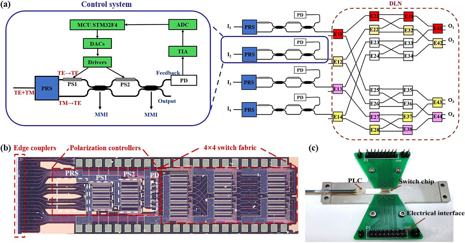
    The detailed structure of the on-chip PC is illustrated in the inset of Fig. 1(a). It is constructed by a PR splitter (PRS)[35], a 2×2 MZI coupler, and a photodetector (PD) at the idle output port of the MZI. The other output port is connected to the 4×4 switch fabric. The PRS is used to split the input light with TE and transverse magnetic (TM) polarizations into two TE branches. The insertion loss and the crosstalk of PRS are 0.35 dB (1.87 dB) and 21dB (13.4dB) for the TE (TM) light, respectively, according to our test device. Thermal PS1 is embedded in the upper branch to control the relative phase between the two branches. The two branches are then connected to an MZI coupler with thermal PS2 embedded in one MZI arm to control the optical power distribution in the two output ports. The on-chip PD is used to convert the optical wave to an electrical signal for feedback control.

    The control system to perform automated polarization adjustment consists of transimpedance amplifiers (TIAs), analog-to-digital converters (ADCs), a micro-control unit (MCU, STM32F4), digital-to-analog converters (DACs), and drivers. The optical signal from the idle output port of the MZI coupler is converted to a photocurrent by the on-chip PD, and then it is amplified by the TIA and sampled by the 12 bit ADC before feedback to the MCU. In the MCU, a polarization control algorithm based on a gradient descent method is implemented to achieve real-time feedback control.

    Figure 1(b) shows the microscope image of the fabricated silicon optical switch chip. The footprint of the chip is 5mm×3mm. We designed a silica-based planar lightwave circuit (PLC) with 2.5% refractive index contrast (Δn) for fiber-to-chip coupling. The PLC waveguide has 3µm×3µm cross-sectional dimensions. The waveguide pitch in the PLC is gradually transformed from 50 µm to 127 µm to accommodate the pitch of a commercial fiber array. The electrical and optical packaging was done in the SJTU-Pinghu Institute of Intelligent Optoelectronics. Figure 1(c) displays the packaged chip.

    3. Simulation and Algorithm

    Using the transfer matrix method, we can derive the normalized optical power at the feedback port of the on-chip PC as a function of phase changes (Δφ1 and Δφ2) of the two PSs:Pf=|12[eiΔφ1(eiΔφ21)eiφTEETEi(eiΔφ2+1)eiφTMETM]|2,where ETE and ETM represent the TE and TM electric field components of the input light before PRS (normalized to the total power, i.e., |ETE|2+|ETM|2=1[36]), respectively, φTE and φTM are the phase changes induced in the PRS. Figure 2 shows the normalized optical power Pf varied with Δφ1 and Δφ2 for different proportions of the input light. The phase difference between the two branches is set to be π/2 as a typical case without losing generality. It can be seen that there are two global minimum points for an arbitrary polarization. We can find the best phase shift values by reaching one of the global minimum points using a control algorithm so that the output power to the switch fabric is maximized.

    Normalized feedback port power Pf as a function of Δφ1 and Δφ2 with different combinations of input polarizations: (a) TE 25%, TM 75%; (b) TE 50%, TM 50%; (c) TE 75%, TM 25%; and (d) TE 100%.

    Figure 2.Normalized feedback port power Pf as a function of Δφ1 and Δφ2 with different combinations of input polarizations: (a) TE 25%, TM 75%; (b) TE 50%, TM 50%; (c) TE 75%, TM 25%; and (d) TE 100%.

    We used a polarization control algorithm based on a gradient descent method to search for the global minimum[34]. Figure 3 shows the algorithm flow chart. Uφ1 and Uφ2 are the applied DAC voltages to PS1 and PS2, respectively. Uf, Uf1, and Uf2 are recorded voltages from the ADC at the feedback port. g1 and g2 represent the gradient of Uf1 and Uf2 updated in each iteration, which determines if the adjustment is in the proper direction. α represents the learning rate, related to the step size of the applied voltages on PS1 and PS2[34]. It is important for the algorithm to select proper parameters, such as the initial values of g1,g2,Uφ1,Uφ2,α, and the threshold voltage Uf_min. Proper initial values can reduce the number of iterations and speed up the adjustment process. Likewise, Uf_min is used to terminate the control loop when the monitored signal is less than the threshold.

    Flow chart of the polarization control algorithm.

    Figure 3.Flow chart of the polarization control algorithm.

    4. Experiments

    To characterize the polarization adjustment of our chip, we first adjusted the on-chip PC in the I2O2 path using the polarization control algorithm described in Fig. 3. A fiber-based commercial PC was inserted between a tunable laser and the optical switch chip to adjust the input polarization state. A digital phosphor oscilloscope (DPO, Tektronix 5054B) was connected to the TIA to capture the output signal at the feedback port. Figures 4(a) and 4(b) show the recorded voltages at the feedback port during the polarization tuning process for two random polarization states. The polarization recovery time is less than 4 ms. We also continuously perturbed the polarization state of the input light by manually adjusting the PC. It can be seen that without automated adjustment, the voltage at the feedback port changes accordingly, as shown in Fig. 4(c), which means that the optical power at the output port varies with the polarization of input light. Figure 4(d) shows the recorded voltages upon active adjustment. The signal at the feedback port is kept at the minimum under a continuously changed input polarization. Therefore, with the on-chip PC, our switch chip can accommodate any dynamically changed input polarization.

    (a), (b) Polarization tuning process for two random polarization states. (c), (d) Recorded TIA voltages with randomly changed input polarization when the algorithm is (c) turned off and (d) turned on.

    Figure 4.(a), (b) Polarization tuning process for two random polarization states. (c), (d) Recorded TIA voltages with randomly changed input polarization when the algorithm is (c) turned off and (d) turned on.

    Figure 5 shows the measured transmission spectra of the I2O2 path after polarization adjustment. The spectra are normalized with a U-shaped reference waveguide. The on-chip insertion loss gradually decreases as the input light polarization rotates from the TE-like to the TM-like state. The PDL is ∼ 2 dB in the wavelength range of 1540 nm–1580 nm. The relatively large PDL is caused by the inverse taper at the input ports of the chip. We also notice that other than these two special polarization states, i.e., TE-like and TM-like states, the spectra show a periodic response with a free spectral range (FSR) of ∼6.6 nm. This is because there is an optical path difference between the two PRS branches in our design.

    Measured transmission spectra of the I2−O2 path for different input polarization states after polarization adjustment.

    Figure 5.Measured transmission spectra of the I2−O2 path for different input polarization states after polarization adjustment.

    Figure 6 shows the measured transmission spectra of one switching state of the optical switch. The four routing paths are I1-O1,I2O2,I3O4, and I4O3, as illustrated by the different colors in Fig. 1(a). Here, we adjusted the PC to maximize the output power while the on-chip PCs were turned off. The on-chip insertion loss of each path is 3.1 dB, 3.5 dB, 6.35 dB, and 6.4 dB at a 1550 nm wavelength, respectively. The worst crosstalk is −10 dB in this state, as shown in Fig. 6(c). The relatively larger insertion loss of paths I3O4 and I4O3 is due to the large insertion loss of switch elements E27 and E28, where a 20 nm lateral alignment error is incurred at the input of the elements in the mask layout design. All sixteen 1×2 MZIs have lateral alignment errors in one of the MZI arms. This slightly increases the insertion loss, but significantly degrades the crosstalk. The insertion loss of path I4O3 is broken down into ∼0.35 dB from the PRS, ∼1.2 dB from three 2×2 MZIs, ∼3.4 dB from one 1×2MZI(E28), ∼0.6 dB from the other 1×2 MZI (E37), and ∼0.85 dB from the crossings and connecting waveguides. Therefore, by correcting the design errors, the insertion loss can be improved to ∼3.2 dB. The crosstalk can also be reduced to ∼−50 dB, as no two optical paths share the same switch element. In Figs. 6(a) and 6(c), periodical ripples are observed in the measured spectra because the input light is not pure TE or TM polarization.

    Measured transmission spectra of one switching state at (a) port O1, (b) port O2, (c) port O3, and (d) port O4.

    Figure 6.Measured transmission spectra of one switching state at (a) port O1, (b) port O2, (c) port O3, and (d) port O4.

    We performed a high-speed on–off keying (OOK) signal transmission experiment with various input polarization states for the I2O2 path. A tunable laser source (TLS) generated a continuous wave (CW) light at the wavelength of 1550 nm. It was then modulated by a commercial modulator. A 32 Gbit/s pseudo-random binary sequence (PRBS) signal with a pattern length of 2311 generated from a pulse pattern generator (PPG, Keysight, N4951B) was used to drive the modulator. The modulated optical signal was amplified by an erbium-doped fiber amplifier (EDFA), and the polarization state of the input light was adjusted by a PC before it was edge-coupled to the switch chip. We used the polarization control system to actively adjust the polarization to the TE mode. The output signal of the switch chip was amplified by another EDFA and followed by an optical bandpass filter. Finally, it was detected by a 50 GHz photodiode (u2t, XPDV2120R) and received by a digital communication analyzer (DCA, Agilent DCA-X 86100D). We measured the eye diagrams for six different input polarization states, as shown in Fig. 7(a). No significant signal degradation was observed from the eye diagrams, indicating high signal integrity after passing the switch chip. These results indicate that the 4 × 4 optical switch chip can achieve polarization-insensitive optical signal routing.

    Optical transmission measurement of a 32 Gbit/s OOK signal for various input polarization states: (a) eye diagrams and (b) BER as a function of received optical power.

    Figure 7.Optical transmission measurement of a 32 Gbit/s OOK signal for various input polarization states: (a) eye diagrams and (b) BER as a function of received optical power.

    To evaluate the optical signal transmission through our optical switch with different input polarization states, we also measured the error-free operation at a bit error rate (BER) of 109 for a 32 Gbit/s OOK signal. Figure 7(b) shows the relationship between the BER and the received optical power (ROP) with the input polarization gradually tuned from TE to TM (POL.1POL.6) mode together with the back-to-back (BTB) measurement as a reference. The ROP is changed by a VOA placed before the photodiode. The power penalty is about 1 dB for the worst polarization state at a BER of 109.

    5. Conclusion

    In conclusion, we have demonstrated a 4×4 polarization-insensitive silicon optical switch based on a dilated DLN architecture. Four on-chip PCs are integrated before the switch fabric for real-time polarization adjustment. The polarization recovery time is less than 4 ms for any arbitrary input polarization state using the polarization control algorithm. The measured PDL is about 2 dB. The 32 Gbit/s OOK data transmission experiment shows that our optical switch can support high-speed data transmission with any input polarization. Our switch offers a new approach to overcome the polarization sensitivity issue to satisfy the practical applications in datacenter networks.

    References

    [1] B. G. Lee, N. Dupuis, P. Pepeljugoski, L. Schares, R. Budd, J. R. Bickford, C. L. Schow. Silicon photonic switch fabrics in computer communications systems. J. Lightwave Technol., 33, 768(2015).

    [2] R. Soref. Tutorial: integrated-photonic switching structures. APL Photon., 3, 021101(2018).

    [3] M. Ma, A. H. K. Park, Y. Wang, H. Shoman, F. Zhang, N. A. F. Jaeger, L. Chrostowski. Sub-wavelength grating-assisted polarization splitter-rotators for silicon-on-insulator platforms. Opt. Express, 27, 17581(2019).

    [4] X. Wang, G. Zhou, Z. Jin, L. Lu, G. Wu, L. Zhou, J. Chen. Wavelength-mode pulse interleaver on the silicon photonics platform. Chin. Opt. Lett., 18, 031301(2020).

    [5] S. Li, R. Cong, Z. He, T. Wang, F. Zhang, S. Pan. Switchable microwave photonic filter using a phase modulator and a silicon-on-insulator micro-ring resonator. Chin. Opt. Lett., 18, 052501(2020).

    [6] Y. Yue, H. Zhu, Z. Cao, J. He, M. Li. Wide-range optical sensors based on a single ring resonator with polarization multiplexing. Chin. Opt. Lett., 17, 031301(2019).

    [7] P. Cheben, R. Halir, J. H. Schmid, H. A. Atwater, D. R. Smith. Subwavelength integrated photonics. Nature, 560, 565(2018).

    [8] Y. Wang, D. Dai. Multimode silicon photonic waveguide corner-bend. Opt. Express, 28, 9062(2020).

    [9] Y. Guo, M. Pu, X. Li, X. Ma, S. Song, Z. Zhao, X. Luo. Chip-integrated geometric metasurface as a novel platform for directional coupling and polarization sorting by spin–orbit interaction. IEEE J. Sel. Top. Quantum Electron., 24, 4700107(2018).

    [10] L. Lu, S. Zhao, L. Zhou, D. Li, Z. Li, M. Wang, X. Li, J. Chen. 16 × 16 non-blocking silicon optical switch based on electro-optic Mach–Zehnder interferometers. Opt. Express, 24, 9295(2016).

    [11] L. Lu, X. Li, W. Gao, X. Li, L. Zhou, J. Chen. Silicon non-blocking 4 × 4 optical switch chip integrated with both thermal and electro-optic tuners. IEEE Photon. J., 11, 6603209(2019).

    [12] K. Tanizawa, K. Suzuki, M. Toyama, M. Ohtsuka, N. Yokoyama, K. Matsumaro, M. Seki, K. Koshino, T. Sugaya, S. Suda, G. Cong, T. Kimura, K. Ikeda, S. Namiki, H. Kawashima. Ultra-compact 32 × 32 strictly-non-blocking Si-wire optical switch with fan-out LGA interposer. Opt. Express, 23, 17599(2015).

    [13] N. Dupuis, B. G. Lee, A. V. Rylyakov, D. M. Kuchta, C. W. Baks, J. S. Orcutt, D. M. Gill, W. M. J. Green, C. L. Schow. Modeling and characterization of a nonblocking 4×4 Mach–Zehnder silicon photonic switch fabric. J. Lightwave Technol., 33, 4329(2015).

    [14] L. Qiao, W. Tang, T. Chu. 32 × 32 silicon electro-optic switch with built-in monitors and balanced-status units. Sci. Rep., 7, 42306(2017).

    [15] N. Sherwood-Droz, H. Wang, L. Chen, B. G. Lee, A. Biberman, K. Bergman, M. Lipson. Optical 4×4 hitless silicon router for optical networks-on-chip (NoC). Opt. Express, 16, 15915(2008).

    [16] D. Nikolova, D. M. Calhoun, Y. Liu, S. Rumley, A. Novack, T. Baehr-Jones, M. Hochberg, K. Bergman. Modular architecture for fully non-blocking silicon photonic switch fabric. Microsyst. Nanoeng., 3, 16071(2017).

    [17] M. Mizukami, J. Yamaguchi, N. Nemoto, Y. Kawajiri, H. Hirata, S. Uchiyama, M. Makihara, T. Sakata, N. Shimoyama, K. Oda. 128×128 three-dimensional MEMS optical switch module with simultaneous optical path connection for optical cross-connect systems. Appl. Opt., 50, 4037(2011).

    [18] T. J. Seok, N. Quack, S. Han, R. S. Muller, M. C. Wu. Large-scale broadband digital silicon photonic switches with vertical adiabatic couplers. Optica, 3, 64(2016).

    [19] T. J. Seok, K. Kwon, J. Henriksson, J. Luo, M. C. Wu. Wafer-scale silicon photonic switches beyond die size limit. Optica, 6, 490(2019).

    [20] S. Han, T. J. Seok, K. Yu, N. Quack, R. S. Muller, M. C. Wu. Large-scale polarization-insensitive silicon photonic MEMS switches. J. Lightwave Technol., 36, 1824(2018).

    [21] H. Fukuda, K. Yamada, T. Tsuchizawa, T. Watanabe, H. Shinojima, S. Itabashi. Silicon photonic circuit with polarization diversity. Opt. Express, 16, 4872(2008).

    [22] D. Dai, L. Liu, S. Gao, D. Xu, S. He. Polarization management for silicon photonic integrated circuits. Las. Photon. Rev., 7, 303(2013).

    [23] K. Suzuki, K. Tanizawa, S.-H. Kim, S. Suda, G. Cong, K. Ikeda, S. Namiki, H. Kawashima. Polarization-rotator-free polarization-diversity 4 × 4 Si-wire optical switch. IEEE Photon. J., 8, 0600707(2016).

    [24] K. Tanizawa, K. Suzuki, K. Ikeda, S. Namiki, H. Kawashima. Non-duplicate polarization-diversity 8 × 8 Si-wire PILOSS switch integrated with polarization splitter-rotators. Opt. Express, 25, 10885(2017).

    [25] A. E. Willner, S. M. R. M. Nezam, L. Yan, Pan Zhongqi, M. C. Hauer. Monitoring and control of polarization-related impairments in optical fiber systems. J. Lightwave Technol., 22, 106(2004).

    [26] D.-X. Xu, P. Cheben, D. Dalacu, A. Delâge, S. Janz, B. Lamontagne, M. J. Picard, W. N. Ye. Eliminating the birefringence in silicon-on-insulator ridge waveguides by use of cladding stress. Opt. Lett., 29, 2384(2004).

    [27] S. Nakamura, S. Yanagimachi, H. Takeshita, A. Tajima, T. Hino, K. Fukuchi. Optical switches based on silicon photonics for ROADM application. IEEE J. Sel. Top. Quantum Electron., 22, 3600609(2016).

    [28] W. N. Ye, D.-X. Xu, S. Janz, P. Cheben, M.-J. Picard, B. Lamontagne, N. G. Tarr. Birefringence control using stress engineering in silicon-on-insulator (SOI) waveguides. J. Lightwave Technol., 23, 1308(2005).

    [29] X. Wang, K. S. Chiang. Polarization-insensitive mode-independent thermo-optic switch based on symmetric waveguide directional coupler. Opt. Express, 27, 35385(2019).

    [30] H. Yang, Q. Cheng, R. Chen, K. Bergman. Polarization-diversity microring-based optical switch fabric in a switch-and-select architecture, Th3B.2(2020).

    [31] K. Suzuki, R. Konoike, N. Yokoyama, M. Seki, M. Ohtsuka, S. Saitoh, S. Suda, H. Matsuura, K. Yamada, S. Namiki, H. Kawashima, K. Ikeda. Nonduplicate polarization-diversity 32 × 32 silicon photonics switch based on a SiN/Si double-layer platform. J. Lightwave Technol., 38, 226(2020).

    [32] K. Sugiyama, T. Chiba, K. Tanizawa, K. Suzuki, T. Kawashima, S. Kawakami, K. Ikeda, H. Kawashima, H. Takahashi, H. Tsuda. Polarization diversity circuit based on silica waveguides and photonic crystal waveplates for a 4×4 silicon optical switch. IEICE Electron. Express, 14, 20170252(2017).

    [33] K. Tanizawa, K. Suzuki, K. Ikeda, S. Namiki, H. Kawashima. Novel polarization diversity without switch duplication of a Si-wire PILOSS optical switch. Opt. Express, 24, 6861(2016).

    [34] M. Ma, H. Shoman, K. Tang, S. Shekhar, N. A. F. Jaeger, L. Chrostowski. Automated control algorithms for silicon photonic polarization receiver. Opt. Express, 28, 1885(2020).

    [35] W. D. Sacher, T. Barwicz, B. J. F. Taylor, J. K. S. Poon. Polarization rotator-splitters in standard active silicon photonics platforms. Opt. Express, 22, 3777(2014).

    [36] R. Cao, Y. He, Q. Zhu, J. Li, S. An, Y. Zhang, Y. Su. Multi-channel 28-GHz millimeter-wave signal generation on a silicon photonic chip with automated polarization control. J. Semiconductors, 40, 052301(2019).

    Xiaorui Li, Liangjun Lu, Wei Gao, Xin Li, Jianping Chen, Linjie Zhou. Silicon non-blocking 4 × 4 optical switch with automated polarization adjustment[J]. Chinese Optics Letters, 2021, 19(10): 101302
    Download Citation