• Journal of Infrared and Millimeter Waves
  • Vol. 39, Issue 2, 157 (2020)
Zhi-Gang LU, Wei-Hua GE, Rui-Dong WEN, Zhi-Cheng SU, Mei-Ling ZHU, Ke-Sen DING, Zhan-Liang WANG, and Tao TANG
Author Affiliations
  • National Key Laboratory of Science and Technology on Vacuum Electronics, School of Electronic Science and Engineering, University of Electronic Science and Technology of China, Chengdu60054, China
  • show less
    DOI: 10.11972/j.issn.1001-9014.2020.02.004 Cite this Article
    Zhi-Gang LU, Wei-Hua GE, Rui-Dong WEN, Zhi-Cheng SU, Mei-Ling ZHU, Ke-Sen DING, Zhan-Liang WANG, Tao TANG. Design and cold-test of sheet beam coupled cavity slow wave structure for W-Band TWT[J]. Journal of Infrared and Millimeter Waves, 2020, 39(2): 157 Copy Citation Text show less

    Abstract

    This paper presents the fabrication and cold-test of a three-slot-staggered-ladder coupled cavity slow wave structure (CC-SWS) along with high power input-output couplers and RF windows in W-band. The SWS is fed by a rectangular waveguide coupler which is made up of a three-order step-transform rectangular waveguide placed on the short edge of the input cavity. Firstly, the dispersion, interaction impedance, transmission property and beam-wave interaction are studied using the simulation method. It is shown that the traveling wave tube (TWT) with a three-slot-staggered-ladder CC-SWS is able to provide a saturation output power of more than 1000 W in the frequency range of 91~96 GHz, and the maximum saturated output power can reach 1125 W at 94 GHz. Secondly, the CC-SWS is fabricated by the high-precision CNC milling and fixed in a nonmagnetic stainless steel housing. Test results of the fabricated CC-SWS with couplers and RF-windows are presented, showing the S11 < -10 dB in the frequency range of 90 GHz to 100 GHz. Therefore, the three-slot-staggered-ladder CC-SWS is a promising slow wave circuit of high power W-band TWT.

    Introduction

    W-band (75∼110 GHz) is a particularly important area for emerging applications, such as high-data-rate communications, high-resolution radar and active imaging, which require high gain and broadband amplifiers with high power levels [1,2]. As a key device, the amplifier critically determines the performance of the whole electronic systems. Due to its outstanding combined performance in power capacity and bandwidth, traveling wave tube (TWT) is one of the most important millimeter wave amplifiers [3,4,5,6,7,8,9,10,11]. Slow wave structure (SWSs) is the key component of TWT amplifier, facilitating efficient interaction between the electromagnetic wave supported by the structure and the electron beam.

    In recent years, folded waveguide (FW) SWS was widely used in the W-band broadband TWT amplifier, and the state-of-the-art output power is more than 250 W in the frequency range of 89.6∼97.6 GHz (8 GHz), with a maximum power of ~424 W and electronic efficiency of ~10% at 92.9 GHz, with beam current of 189-mA and beam voltage of 22.5-kV [12]. However, the further increase of output power is severely limited by the current that can be propagated through the device at this voltage, by the power loading on the circuit, and by issues of the circuit stability. Distributed beams, i.e., multiple or sheet beams, offer the prospect of significantly higher electron current, and hence power, with no increase in the operating voltage. Double-staggered-grating (DSG) SWS for sheet beam was proposed and used in the sheet beam TWT amplifier in W-band. At present, the state-of-the-art output power approaches 644 W at 94 GHz with a corresponding gain of 38.1 dB [13]. Both FW-SWS and SDG-SWS have the characteristics of all-metal, ease fabricated, low operating voltage, but the fatal obstacle is that the low interaction impedance limits the further improvement of output power.

    In order to obtain higher output power, a sheet beam CC-SWS, called three-slot-staggered-ladder CC [
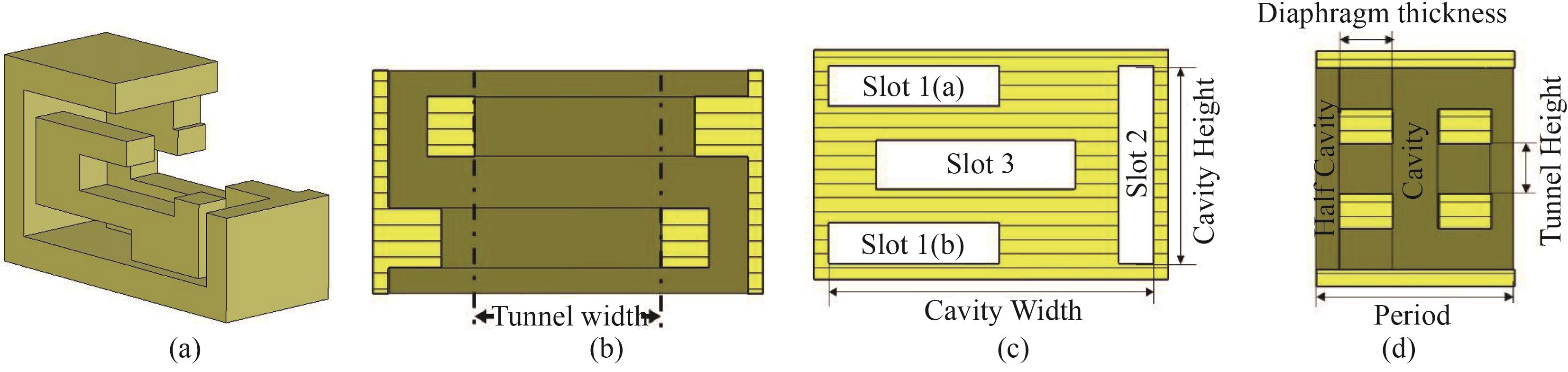
14,15,16], was applied to W-band TWT for the first time. Three-slot-staggered-ladder CC-SWS had been shown to strike a good balance between high power and broadband capability. A generic design for one cell of the structure is shown in Fig. 1. It consists of two rectangular half cavities separated by a septum with a beam tunnel and three coupling slots; the cavity is constructed without ferrules. The adjacent cells are rotated 180° around the beam-tunnel axis (which is the same as being mirrored the long way) so that the beam tunnel stays in the same position and Slot 2 of the next cell is on the right side of the beam tunnel (looking down along the direction of electron travel). From the Fig.1, the size of CC-SWS is so small that it cannot be machined by the integrated fabrication technology which is mainly used to fabricate FW-SWS and SDG-SWS. So the single metal-diaphragm of three-slot-staggered-ladder CC-SWS, as shown in Fig.1(b), is firstly machined by the high-precision CNC milling, and then assembled and welded under the microscope. What we have to pay special attention to here is that cumulative errors caused by diaphragm-assembly must be considered. So far the experimental study on a W-band three-slot-staggered-ladder CC-TWT circuit has not been reported. In this paper, we discuss the fabrication technology and cold-test according to the simulation results of the three-slot-staggered-ladder CC-SWS, which is the first demonstration of the application of sheet beam CC-SWS in W-band TWT.

    (a) Cut-away isometric view of a 3-D model of a full period (created by stacking two rotated unit cells), (b) the top view, (c) the left view, and (d) the front view of cutting-plane of the full period three-slot SWS

    Figure 1.(a) Cut-away isometric view of a 3-D model of a full period (created by stacking two rotated unit cells), (b) the top view, (c) the left view, and (d) the front view of cutting-plane of the full period three-slot SWS

    1 Design and simulation

    The dispersion and interaction impedance of the sheet beam CC-SWS with parameters listed in Table 1 were obtained by the simulating method using the Ansoft HFSS. The fundamental harmonic of the first mode is backward wave for this type of circuit, so the first spatial harmonic is selected to interact with electron beam, as shown in Fig. 2(a). And an unconventional mode 2 appears in the dispersion diagram due to the introduction of wide sheet beam tunnel. In order to reduce mode competition, the electron beam tunnel must not be too wide. The normalized phase velocity versus frequency of the fundamental mode at the first spatial harmonic is also given in Fig. 2(b). It shows that the dispersion curve is relatively flat over a broad bandwidth. And the phase velocity determines the beam voltage, which is approximately 22 kV here, required for synchronized interaction with the electron beam.

    Parametermm
    Period1.2
    Slot 1 & 2 width0.25
    Slot 1 & 2 length1.22
    Slot 3 width0.3
    Slot 3 length1.42
    Cavity width2.32
    Cavity height1.22
    Beam tunnel
    width1.2
    height0.30
    Diaphragm thickness0.32

    Table 1. Parameters for simulated SWS

    Dispersion curves of the sheet beam CC-SWS (a) frequency varies with phase shift, (b) normalized phase velocity varies with frequency

    Figure 2.Dispersion curves of the sheet beam CC-SWS (a) frequency varies with phase shift, (b) normalized phase velocity varies with frequency

    As a measure of the beam-wave interaction strength, the interaction impedance over cross-section of the sheet beam is also calculated using the Ansoft HFSS. First, the distribution of interaction impedance on the cross-section of beam tunnel is analyzed, and given as shown in Fig. 3(a). Secondly, according to the distribution of interaction impedance on the cross-section of sheet beam in Fig. 3(b), the position and size of electron beam are determined, and the average interaction impedance on the cross-section of sheet beam is calculated and shown in Fig. 3 (c). Compared with the CC-SWS using the circular electron beam, the interaction impedance is basically at the same level [17], and the interaction impedance of three-slot-staggered-ladder CC-SWS is much higher than that of the FW-SWS and SDG-SWS [12,13]. The sheet beam can increase the DC input power by distributing the beam current over an increasing area, which indicates that the sheet beam CC-TWT can obtain higher output power.

    The distribution of interaction impedance on (a) the cross-section of beam tunnel, (b) the cross-section of sheet beam, and (c) average interaction impedance over the cross-section of sheet beam

    Figure 3.The distribution of interaction impedance on (a) the cross-section of beam tunnel, (b) the cross-section of sheet beam, and (c) average interaction impedance over the cross-section of sheet beam

    Impedance matching between the CC-SWS and input-output waveguide is important for signal transmission, which can improve tube efficiency, gain and stability over the required bandwidth. The transmission model of the sheet-beam CC-SWS including the main section, input/output couplers and RF windows is present, as shown in Fig. 4(a). The coupler is a three-order step-transform rectangular waveguide placed on the short edge of the input/output cavity. The optimal design of coupler for sheet-beam CC-SWS is obtained using the time-domain solver in the CST Microwave Studio. The simulation results of transmission characteristics are given in Fig. 4(b). The reflection parameter S11 is almost below -20 dB in the frequency range of 91.2∼100.7 GHz.

    (a) The vacuum model, and (b) the transmission characteristics of the sheet beam CC-SWS

    Figure 4.(a) The vacuum model, and (b) the transmission characteristics of the sheet beam CC-SWS

    A 3-D particle-in-cell (PIC) model of sheet-beam CC-TWT is constructed. The beam-wave interaction simulations are carried out by using the PIC solver in CST Particle Studio to substantiate the amplification capability of the TWT. In the simulation, the cross-section size of sheet beam is set as 0.72 mm0.18 mm. The synchronous voltage is 22 kV and the current of 500 mA. According to the beam tunnel size of 1.2 mm0.3 mm, the filling ratio is 36% (60% in both x- and y-coordinates), then the current density of sheet beam is 379 A/cm2. In order to make the sheet beam propagate stably and not be intercepted by the slow wave circuit, a 0.8 Tesla uniform solenoidal magnetic field is used for beam focusing. In addition, it should be noted that the saturated gain of the whole TWT is low (less than 20 dB generally), so the length of the tube can be further shortened to ensure the stable transmission of the sheet beam with such high current density. In the following calculation, the saturated gain and length of sheet-beam CC-TWT are given. The material of SWS circuit is set as oxygen-free copper, and its conductivity is 2.25107 S/m, which means the distribution loss and surface roughness of the circuit is considered. The typical simulation results at the center frequency of 94 GHz are exhibited in Fig.5,6,7,8.

    The electron bunching phenomenon at 94 GHz

    Figure 5.The electron bunching phenomenon at 94 GHz

    Phase momentum of bunched electron beam at 94 GHz

    Figure 6.Phase momentum of bunched electron beam at 94 GHz

    Input and output signals at 94 GHz

    Figure 7.Input and output signals at 94 GHz

    Frequency spectrum of output signal at 94 GHz

    Figure 8.Frequency spectrum of output signal at 94 GHz

    All of the electrons are well confined in the beam tunnel, with no electron intercepted, and the electron bunching phenomenon around the end of the circuit is given, as shown in Fig. 5. According to the Fig. 5, the accelerating electrons and retarding electrons are periodically arranged along the longitudinal direction, which demonstrates a good beam-wave energy exchange process. Fig.6 shows the phase momentum plot of the bunched electron beam along the longitudinal distance when the electron dynamic system has been in steady state. As the electron beam propagates along the circuit, most of the electrons experience a continuous deceleration along the slow-wave circuit. This continuous interaction results in a continuously increasing wave amplitude at the output port of the TWT, as depicted in Fig. 7. The power at output port becomes stable at 1125 W, corresponding to the gain of 15.75 dB without oscillation. Fig.8 gives the frequency spectrum of output signal. As for the output signal, the spectrum is relatively pure. Although the higher harmonics are also aroused, the amplitudes are much lower than that of the operating frequency of 94 GHz.

    According to the same method, the TWT at each frequency can be driven to the saturated state by adjusting the input power. The plot of saturated output power versus frequency in the frequency range of 91∼96 GHz is shown in Fig. 9(b). The designed sheet-beam CC-TWT can produce saturated output power of more than 1000 W in the frequency range of 91∼96 GHz, and the corresponding saturated gain can reach over 15 dB. The maximum saturated output power can reach 1125 W at 94 GHz. The saturated electron efficiency is greater than 8.52% across the frequency range of 91∼96 GHz.

    (a) The electron efficiency and saturated gain, and (b) the saturated output power versus the frequency

    Figure 9.(a) The electron efficiency and saturated gain, and (b) the saturated output power versus the frequency

    2 Fabrication and cold-test

    The W-band three-slot-staggered-ladder CC-TWT circuit was fabricated by using the traditional machining method, where the circuit is milled by a micromachining high speed CNC mill. The size of the CC-diaphragm is 2.32 mm1.22 mm, and three grooves as well as the beam tunnel are opened on the diaphragm. The structural dimensions are very small, and it is difficult to fabricate using the common oxygen-free copper. Here the special oxygen-free copper is used to fabricate the diaphragm. Meanwhile in order to reduce the superposition error, the accuracy of each coupled-cavity diaphragm thickness is strictly controlled within a certain range. Each piece is numbered and assembled in order. The fabricated coupled-cavity diaphragms, transition waveguides and input & output window components are shown in Fig.10.

    (a) Coupled-cavity diaphragms, (b) transition waveguides, and (c) input & output window components

    Figure 10.(a) Coupled-cavity diaphragms, (b) transition waveguides, and (c) input & output window components

    To test the transmission characteristics of the W-band three-slot-staggered-ladder CC-TWT circuit, the clamping molds are designed to assemble and fix the components of the CC-SWS diaphragms. The test sample is shown in Fig. 11. For the CC-SWS (20 cycles) tested in this paper, the measured cumulative error is 0.06 mm (the machining accuracy is 0.005 mm, the maximum cumulative error is 0.1 mm).

    (a) Clamping molds and the final test sample, (b) assembly drawing using UG software, and (c) assembly for testing

    Figure 11.(a) Clamping molds and the final test sample, (b) assembly drawing using UG software, and (c) assembly for testing

    Figure 12 shows the test site. The Vector Network Analyzer (VNA) is used to test the S parameters and voltage standing wave ratio (VSWR) of three-slot-staggered-ladder CC-TWT circuit. Here, two 90-degree bend-waveguides are used to connect to two S-parameter spread spectrum modules of VNA, respectively. The test result of the parameter S11 is shown in Fig.13, which shows that magnitude of reflection signal is less than -10 dB over the frequency range of 90∼100 GHz. According to the test results, the VSWR is deduced and shown in Fig. 14. At the same time, as a comparison, the simulation results of S11 and VSWR are also plotted on the Fig.13 and Fig. 14. It can be seen that the simulation results are not in good agreement with the test results. For W-band SWS, the machining accuracy of 0.005 mm is far enough to meet the manufacturing requirements. The errors of simulation and test results are mainly caused by assembly and welding. Assembly error is inevitable and can only be improved by the technology of technicians. For the welding, only the I/O waveguide is welded, the coupled-cavity diaphragms are too small to be welded, so the mold is used to fix them, as shown in Fig. 11. The electromagnetic wave can leak out through the tiny gap between the coupled-cavity diaphragms, which is the main reason for the error between the test and simulation results. In the future, a stainless steel sleeve can be used to seal the diaphragms, which is an effective way to solve the welding error.

    Test site of the CC-TWT circuit

    Figure 12.Test site of the CC-TWT circuit

    S11 comparison between cold-test and simulation results

    Figure 13.S11 comparison between cold-test and simulation results

    VSWR comparison between test and simulation results

    Figure 14.VSWR comparison between test and simulation results

    3 Conclusion

    The design of sheet beam CC-TWT with a single-section SWS was carried out. The piece parts of three-slot-staggered-ladder CC-SWS, couplers and RF windows were fabricated and assembled. Cold tests were carried out to characterize the three-slot-staggered-ladder CC-SWS and the RF windows. The measured S-parameter S11 is less than -10 dB in the frequency range of 90-100 GHz. These results lay the foundation for the realization of the W-band three-slot-staggered-ladder CC-TWT.

    References

    [1] R H Abrams, B Levush, A A Mondelli. Vacuum electronics for the 21st century. IEEE Microwave Magazine, 2, 61-72(2001).

    [2] J H Booske, R J Dobbs, C D Joye. Vacuum electronic high power terahertz sources, 1, 54-75(2011).

    [3] S M Wang, S Aditya, J Miao. Design of a sheet-beam electron-optical system for a micro fabricated W-band traveling-wave tube using a cold cathode. IEEE Transaction on Electron Devices, 63, 3725-3732(2016).

    [4] S Fang, J Xu, H R Yin. Experimental verification of the low transmission loss of a flat-roofed sine waveguide slow-wave structure. IEEE Electron Device Letters, 40, 808-811(2019).

    [5] Z Lu, W Ge, R Wen. High power folded waveguide traveling wave tube based on variable-width technology. Physics of Plasma, 26, 31061-31067(2019).

    [6] A M Cook, C D Joye, J P Calame. W-Band and D-Band traveling-wave tube circuits fabricated by 3D printing. IEEE Access, 7, 72561-72566(2019).

    [7] A Srivastava, V L Christie. Design of a high gain and high efficiency W-band folded waveguide TWT using phase-velocity taper. Journal of Electromagnetic Waves and Applications, 32, 1316-1327(2018).

    [8] M Mineo, A D Carlo, C Paoloni. Analytical design method for corrugated rectangular waveguide SWS THz vacuum tubes. Journal of Electromagnetic Waves and Applications, 24, 2479-2494(2010).

    [11] F Malek. The analytical design of a folded waveguide traveling wave tube and small signal gain analysis using Madey's theorem. Progress in Electromagnetics Research, 98, 137-162(2009).

    [12] X Zhang, J Feng, J Cai. Design and experimental study of 250-W W-band pulsed TWT with 8 GHz bandwidth. IEEE Transaction on Electron Device, 64, 5151-5156(2017).

    [13] Y Fan, J Luo, Z Fang. W-band sheet beam staggered double grating traveling wave tube with simplified input output structure:Proceeding of International Vacuum Electronics Conference, London, 2017, 1-2(2017).

    [14] P B Larsen, D K Abe, S J Cooke. Characterization of a Ka-band sheet beam coupled cavity slow wave structure. IEEE Transaction on Plasma Science, 38, 1244-1254(2010).

    [15] D E Pershing, K T Nguyen, D K Abe. Demonstration of a wideband 10-kW Ka-band sheet beam TWT amplifier. IEEE transaction on Electron Devices, 61, 1637-1642(2014).

    [16] Z Su, Z Lu, Z Wang. Preliminary design of a three-slot-staggered-ladder coupled-cavity structure for W-band pulse power traveling wave tube: Proceeding of International Vacuum Electronics Conference, Montery, 2018, 131-132(2018).

    [17] Y Liu, Y Gong, Y Wei. Design of a 100 W V-band coupled cavity traveling wave tube: China-Japan Joint Microwave Conference, Hangzhou, 2011, 458-460(2011).

    Zhi-Gang LU, Wei-Hua GE, Rui-Dong WEN, Zhi-Cheng SU, Mei-Ling ZHU, Ke-Sen DING, Zhan-Liang WANG, Tao TANG. Design and cold-test of sheet beam coupled cavity slow wave structure for W-Band TWT[J]. Journal of Infrared and Millimeter Waves, 2020, 39(2): 157
    Download Citation