
Hexi Liang, Tianhao Shen, Zhenya Wang, Cong Cao, Yun Xiao, Yong Ai. Research and design of underwater wireless optical communication system with dual light sources[J]. Infrared and Laser Engineering, 2021, 50(9): 20200445
- Infrared and Laser Engineering
- Vol. 50, Issue 9, 20200445 (2021)
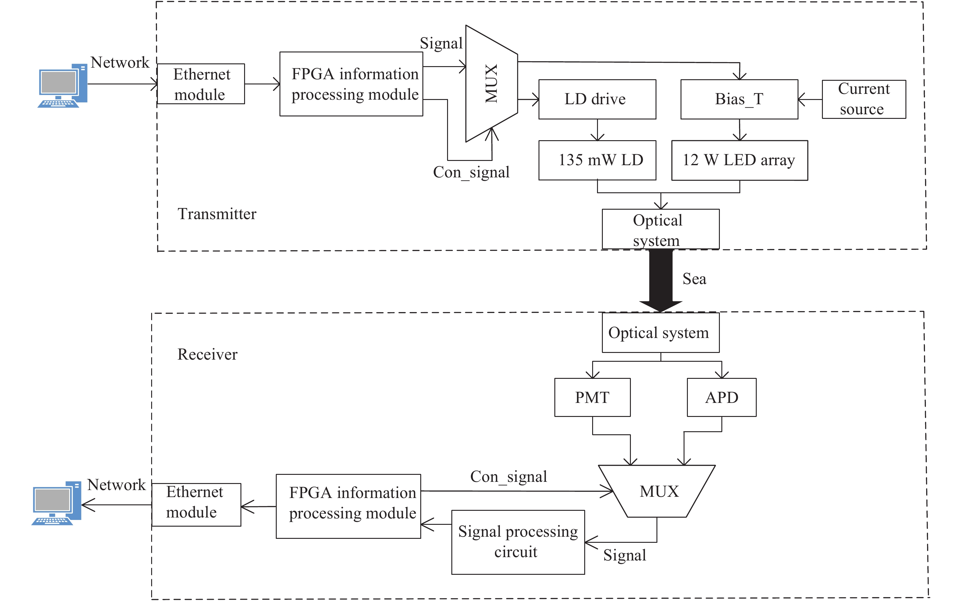
Fig. 1. Overall structure diagram of the system
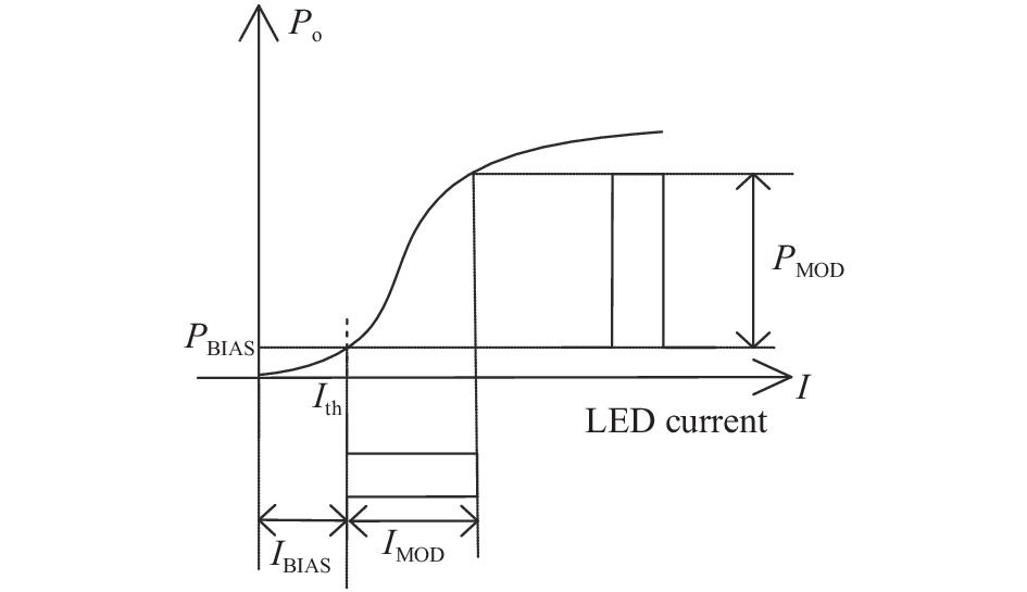
Fig. 2. LED digital modulation characteristic curve
Fig. 3. Improved circuit model diagram
Fig. 4. Schematic diagram of high-power LED signal modulation circuit
Fig. 5. Measured value of the current flow through the LED
Fig. 6. 5 MHz waveform of APD receiving communication bandwidth
Fig. 7. Schematic diagram of the receiving end of the system
Fig. 8. APD detector 45 MHz test output signal
Fig. 9. PMT detector 45 MHz test output signal
Fig. 10. FPGA control core block diagram
Fig. 11. FPGA control unit encoding and decoding data flow
Fig. 12. Underwater optical communication link model
Fig. 13. Engineering prototype
Fig. 14. Underwater experiment test scenario
Fig. 15. Simulating underwater test experiment
Fig. 16. Bit error rate performance test of equipment
Fig. 17. Upper computer display transceiver data diagram
|
Table 1. Comparison table of performance parameters between traditional OOK modulation mode and improved OOK modulation mode
|
Table 2. Wireless optical transmission characteristic parameters of underwater equipment
|
Table 3. Equipment performance parameter test


Set citation alerts for the article
Please enter your email address

© Copyright 2018-2021 | Chinese Laser Press. All Rights Reserved 沪ICP备15018463号-20