
Xin-Tao He, Meng-Yu Li, Hao-Yang Qiu, Wen-Sheng Ruan, Li-Dan Zhou, Lin Liu, Xiao-Dong Chen, Wen-Jie Chen, Fu-Li Zhao, Jian-Wen Dong, "In-plane excitation of a topological nanophotonic corner state at telecom wavelengths in a cross-coupled cavity," Photonics Res. 9, 1423 (2021)
- Photonics Research
- Vol. 9, Issue 8, 1423 (2021)
Abstract
1. INTRODUCTION
The optical cavity mode is a fundamental mechanism for light manipulation and light–matter interaction at nanoscale [1]. In silicon photonics, the implementation of passive devices, such as on-chip optical filters, routers, and multiplexers, is highly relevant to the control capability of cavity modes. A photonic crystal (PC) slab provides a useful tool to manipulate cavity modes in silicon photonic integrated circuits (PICs), through finely engineering point defects in the precise location of the PC slab [2,3]. This local method enables us to flexibly control the cavity modes in an extrinsic way, along with increasing the design complexity. Due to recent advances of topological photonics [4–6], a 2D PC slab provides a standard and advanced platform to experimentally explore a variety of topological crystalline phases that are difficult to implement in atomic scale [7–13], and gives a new paradigm to design novel devices in PICs [14–19]. One can apply the simple topology language to achieve an intrinsic cavity mode with a global method [17,20] (i.e., the cavity mode will be induced by the global feature of topological bulk states). In other words, such an intrinsic cavity mode is totally predictable by investigating the bulk topology, regardless of the local region of PC slab.
In 2D topological photonics [21,22], there are two strategies to design an optical cavity. One is the first-order topological phase that a 2D PC with 2D insulating bulk states supports 1D topological edge states. Due to the robust propagation of edge states along the sharp-bending interface, it is possible to achieve a whispering-gallery-mode ring cavity with an arbitrary profile [20,23,24]. Another is the second-order topological phase, in which a 2D PC with a 2D insulating bulk states supports 0D topological corner states [25–31]. Such 0D corner states with in-plane localization will induce a small-mode-volume cavity mode, and thus the cavity size can be reduced for miniaturization. Nowadays, based on III–V semiconductor materials, the second-order topological photonic crystal (SOTPC) slab has been extensively explored for light–matter interaction [17,32–35], such as light emission of quantum dots, lasing, and quantum electrodynamics. On the other hand, exploration of second-order corner states in silicon PICs is important for the design of a cavity and its passive devices. To do this, two main issues must be overcome: (i) how to quantitatively determine the second-order topological phase (i.e., bulk polarization) in a PC slab, and (ii) how to experimentally couple the corner state by propagating waves along waveguides (i.e., in-plane excitation), so it can be compatible with other integrated devices.
In this work, a physics quantity of Bloch-mode symmetry with respect to a mirror-flip operation is proposed to evaluate the bulk polarization of SOTPC in theory, and to experimentally observe the topological nanophotonic corner state in a cross-coupled cavity at a telecommunications wavelength. Two types of dielectric-vein PCs, with topologically distinct bulk polarizations, are designed on a standard silicon-on-insulator (SOI) platform that allows integration with other optoelectronic devices in a silicon PIC. In simulation, the nanophotonic corner state in a 90-deg-bend interface constructed by such two topologically distinct PCs is characterized by the local density of state spectra, mode pattern, and 2D spatial Fourier transformation. To experimentally observe the corner state, we fabricate a cross-coupled PC cavity based on the bend interface of SOTPC and image the corner state via a far-field microscope. In addition, we measure the transmission spectra of the interface to characterize the cross-coupled cavity property via a temporal coupled-mode theory.
Sign up for Photonics Research TOC. Get the latest issue of Photonics Research delivered right to you!Sign up now
2. RESULTS
A. Second-Order Topological Photonic Crystal in a Silicon Membrane
Here, the second-order topological structure is designed by a dielectric-vein PC, whose unit cell consists of four square-hole clusters in a silicon background, as shown in Fig. 1. In theory, such an SOTPC can be preliminarily described by the 2D Su–Schrieffer–Heeger (SSH) model [36,37], which gives a clear picture to analyze the intrinsic mechanism. The topology of SOTPC is related to the mirror symmetry of its eigenfields at high-symmetry
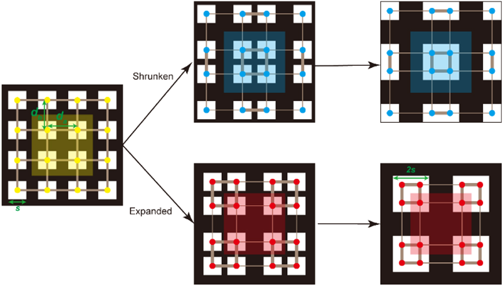
Figure 1.2D Su–Schrieffer–Heeger (SSH) model to describe SOTPCs with four square-holes clusters. To shrink/expand the clusters to the center/corner of unit cell, the structure will generate inequivalent inter-intra hopping (
In SOTPC design, we consider a dielectric-vein PC slab based on a free-standing silicon membrane (the refractive index of silicon is
![]()
Figure 2.Bulk states of SOTPC in a silicon membrane. (a) 3D schematic of the designed SOTPC in free-standing silicon membrane with 220 nm thickness. It can be viewed as a dielectric-vein PC in a square lattice with the periodicity
We should emphasize that the topology of an expanded PC is quite different from that of a shrunken PC, although they share the same band structure. Such second-order topological phase can be characterized by bulk polarization
To determine the second-order topological phase in PCs, a general method is to “see” the eigenmode distributions and qualitatively judge the parity at high-symmetry
B. Localized Cavity Mode Based on the Topological Corner State
For the second-order topological phase, one essential feature is that a 2D PC with nontrivial bulk polarization supports a 0D topological corner state. As schematically shown in Fig. 3(a), when considering a 90-deg-bend interface constructed by shrunken (blue) and expanded (red) PCs, the corner state will be induced by the differences in bulk polarizations.
![]()
Figure 3.Localized cavity mode based on topological corner state in a 90 deg bend interface. (a) Schematic illustration of a bend interface constructed by shrunken (blue) and expanded (red) PCs. (b) Photonic LDOS spectrum at the corner point of the bend interface, which is normalized by the LDOS in vacuum. (c)
To confirm the corner state in simulation, a general method is used to distinguish the eigenmode of corner state from other eigenmodes within the bandgap. This method is applicable for the 2D model, whereas it is not as straightforward to be generalized into a 3D PC slab because the corner state in a PC slab is buried in lots of additional air modes. On the other hand, the corner state is a high-
Next, we will focus on the resonant mode distributions in both the real space and momentum space. Figure 3(c) gives the
C. Far-Field Microscope Images of the Corner State in a Cross-Coupled Cavity
In the experiment, one of the key issues is how to excite the 3D-confined corner state. This work aims to discuss in-plane excitation of the topological corner state in an SOI platform, which is promising for integrated passive devices. As shown in Fig. 4(a), we design a cross-coupled cavity based on the SOTPC bend interface, of which some edge rectangular holes are filled with silicon to form a line-defect photonic crystal waveguide (PCW). The incident waves propagate along the strip waveguide (waveguide width
![]()
Figure 4.Experimental observation of nanophotonic corner states through far-field images. (a) Schematic view and (b) SEM images of cross-coupled cavity based on the bend interface of SOTPC. Note that some edge rectangular holes are filled with silicon to form a line-defect photonic crystal waveguide. (c) Far-field images of bulk, edge, and corner states in a cross-coupled cavity sample via an optical microscope system. (d) Simulated field patterns of electromagnetic energy of bulk, edge, and corner states at the
For optical testing, a fiber-to-chip alignment system with a far-field microscope is applied to characterize the topological nanophotonic corner state (see Appendix A.3). A near-IR (NIR) continuous wave was firstly launched into a fiber polarizer to select the TE mode, and then coupled to the device with the aid of a lensed fiber. After passing through device, the out-of-plane radiation signals were collected by a
D. Q-Factor Measurement of the Corner State in a Cross-Coupled Cavity
Apart from the far-field observation of the corner state, it is necessary to deeply study the optical properties and coupling mechanism of the cross-coupled cavity. In this section, we will use the temporal coupled-mode theory (CMT) [2,43,44] to further study the optical properties of the above cross-coupled cavity, which can be modeled as shown in the schematic diagram of Fig. 5(a). In CMT, the cavity mode with field amplitude
![]()
Figure 5.Measurement of transmission spectra and
In the experiment, Fig. 5(c) gives the SEM images of fabricated samples for bulk crystal, a flat interface, and cross-coupled cavity, respectively. The shrunken/expanded PCs are labeled as blue/red false color. The measured transmission spectra of bulk crystal (black), flat interface (blue), and cross-coupled interface (red) samples are shown in Fig. 5(d), which is normalized by the transmission spectra of a strip Si waveguide. In the low-transmission region of bulk crystal and flat interface, the spectrum of the cross-coupled cavity has a resonant peak near 1383 nm, in correspondence with the corner state. Around the resonant wavelength, we show another measured transmission spectrum of the cross-coupled cavity normalized by the transmittance of a line-defect PCW, as the red dots shown in Fig. 5(e). Based on CMT, we obtain a Lorentz fitting curve (green) to experimentally evaluate the resonant wavelength
3. CONCLUSION
In summary, we have successfully implemented a cross-coupled PC cavity based on second-order topology and observed a topological corner state under in-plane excitation at a telecommunications wavelength. Both simulated results in the bend interface and measured results in the cross-coupled PC cavity show evidence of the topological corner state in silicon PIC. In addition, we measure the transmission spectra of the interface to characterize the optical property of the cross-coupled cavity, and retrieve the intrinsic
APPENDIX A: METHODS
All of simulation results in this work are retrieved from a suspended slab in 3D model. The maximum scale of the discrete grid is smaller than 27?nm, making the resolution large enough to ensure the convergence.
By using the eigenmode solver of the MIT Photonic Bands (MPB) [
On the other hand, all of the calculations for the
The experimental samples were manufactured by employing a top-down nanofabrication process on an SOI wafer (with a nominal 220?nm device layer and 2.0?μm buried oxide layer). First, a 370?nm thickness positive resist (ZEP520A) was spun with a rotating speed of 3500?min?1 on the wafer, and dried for 10?min at 180?°C. The PC patterns were defined by electron-beam lithography (EBPG5000 ES, Vistec) in the resist, and developed by dimethylbenzene for 70?s. Second, an inductively coupled plasma (ICP) etching step was applied to etch the PC structures and coupling waveguides on the top 220?nm thick silicon layer. Then the resist was removed by using an ultrasonic treatment process at room temperature. The final step was to hollow out the substrate
Figure?
![]()
Figure 6.Schematic diagram of the experimental setup.
APPENDIX B: OPENING THE PHOTONIC BANDGAP BY CLUSTER SHRINKAGE/EXPANSION
The unit cell of photonic crystal (PC) in this work consists four air-hole clusters in the silicon background, as depicted in Fig.?
![]()
Figure 7.Evolution of photonic band structures with cluster shrinkage/expansion. (a) Schematic view of the photonic crystal unit cell, consisting of four air-hole clusters. (b)–(d) TE band structures with different intra-cluster distance.
To simplify, the band structures in this section are calculated from a 2D effective model with the background refractive index
In PCs, it is common sense that the spatial Fourier components of cavity mode are related to the origin of bandgap opening. For our case shown in Fig.?
APPENDIX C: DETAILS FOR FAR-FIELD IMAGES OF THE CROSS-COUPLED CAVITY
In this section, we will show more details about the experiments of cross-coupled cavity. The far-field microscope images in Figs.?
![]()
Figure 8.Far-field images of cross-coupled cavity, under in-plane excitation of (a) bulk state at
APPENDIX D: TEMPORAL COUPLED-MODE THEORY
Here is a detailed deduction about the temporal coupled-mode theory (CMT) for the description of our cross-coupled cavity. The CMT model is schematically shown in the main text in Fig.?
For simplification, we consider three conditions. (1) In a linear system, the frequency is conserved, so that the field should oscillate as time-harmonic form
Therefore, the transmission spectrum can be retrieved as
It means the transmittance is a Lorentz profile as a function of
To retrieve the transmission spectrum in the simulation and experiment, we should obtain the input power
References
[1] K. J. Vahala. Optical microcavities. Nature, 424, 839-846(2003).
[2] J. D. Joannopoulos, S. G. Johnson, J. N. Winn, R. D. Meade. Photonic Crystals: Molding the Flow of Light(2011).
[3] Y. Akahane, T. Asano, B.-S. Song, S. Noda. High-
[4] F. Haldane, S. Raghu. Possible realization of directional optical waveguides in photonic crystals with broken time-reversal symmetry. Phys. Rev. Lett., 100, 013904(2008).
[5] L. Lu, J. D. Joannopoulos, M. Soljacic. Topological photonics. Nat. Photonics, 8, 821-829(2014).
[6] T. Ozawa, H. M. Price, A. Amo, N. Goldman, M. Hafezi, L. Lu, M. C. Rechtsman, D. Schuster, J. Simon, O. Zilberberg, I. Carusotto. Topological photonics. Rev. Mod. Phys., 91, 015006(2019).
[7] L.-H. Wu, X. Hu. Scheme for achieving a topological photonic crystal by using dielectric material. Phys. Rev. Lett., 114, 223901(2015).
[8] Y. Yang, Y. F. Xu, T. Xu, H. X. Wang, J. H. Jiang, X. Hu, Z. H. Hang. Visualization of a unidirectional electromagnetic waveguide using topological photonic crystals made of dielectric materials. Phys. Rev. Lett., 120, 217401(2018).
[9] J.-W. Dong, X.-D. Chen, H. Zhu, Y. Wang, X. Zhang. Valley photonic crystals for control of spin and topology. Nat. Mater., 16, 298-302(2017).
[10] T. Ma, G. Shvets. All-Si valley-Hall photonic topological insulator. New J. Phys., 18, 025012(2016).
[11] X.-D. Chen, F.-L. Zhao, M. Chen, J.-W. Dong. Valley-contrasting physics in all-dielectric photonic crystals: orbital angular momentum and topological propagation. Phys. Rev. B, 96, 020202(2017).
[12] X.-D. Chen, W.-M. Deng, F.-L. Shi, F.-L. Zhao, M. Chen, J.-W. Dong. Direct observation of corner states in second-order topological photonic crystal slabs. Phys. Rev. Lett., 122, 233902(2019).
[13] B.-Y. Xie, G.-X. Su, H.-F. Wang, H. Su, X.-P. Shen, P. Zhan, M.-H. Lu, Z.-L. Wang, Y.-F. Chen. Visualization of higher-order topological insulating phases in two-dimensional dielectric photonic crystals. Phys. Rev. Lett., 122, 233903(2019).
[14] S. Barik, A. Karasahin, C. Flower, T. Cai, H. Miyake, W. DeGottardi, M. Hafezi, E. Waks. A topological quantum optics interface. Science, 359, 666-668(2018).
[15] X. T. He, E. T. Liang, J. J. Yuan, H. Y. Qiu, X. D. Chen, F. L. Zhao, J. W. Dong. A silicon-on-insulator slab for topological valley transport. Nat. Commun., 10, 872(2019).
[16] M. I. Shalaev, W. Walasik, A. Tsukernik, Y. Xu, N. M. Litchinitser. Robust topologically protected transport in photonic crystals at telecommunication wavelengths. Nat. Nanotechnol., 14, 31-34(2019).
[17] Y. Ota, F. Liu, R. Katsumi, K. Watanabe, K. Wakabayashi, Y. Arakawa, S. Iwamoto. Photonic crystal nanocavity based on a topological corner state. Optica, 6, 786-789(2019).
[18] Y. Yang, Y. Yamagami, X. Yu, P. Pitchappa, J. Webber, B. Zhang, M. Fujita, T. Nagatsuma, R. Singh. Terahertz topological photonics for on-chip communication. Nat. Photonics, 14, 446-451(2020).
[19] Y. Yang, Z. Jia, Y. Wu, R.-C. Xiao, Z. H. Hang, H. Jiang, X. C. Xie. Gapped topological kink states and topological corner states in honeycomb lattice. Sci. Bull., 65, 531-537(2020).
[20] B. Bahari, A. Ndao, F. Vallini, A. El Amili, Y. Fainman, B. Kanté. Nonreciprocal lasing in topological cavities of arbitrary geometries. Science, 358, 636-640(2017).
[21] A. B. Khanikaev, G. Shvets. Two-dimensional topological photonics. Nat. Photonics, 11, 763-773(2017).
[22] M. Kim, Z. Jacob, J. Rho. Recent advances in 2D, 3D and higher-order topological photonics. Light Sci. Appl., 9, 130(2020).
[23] D. Smirnova, A. Tripathi, S. Kruk, M. S. Hwang, H. R. Kim, H. G. Park, Y. Kivshar. Room-temperature lasing from nanophotonic topological cavities. Light Sci. Appl., 9, 127(2020).
[24] Z.-Q. Yang, Z.-K. Shao, H.-Z. Chen, X.-R. Mao, R.-M. Ma. Spin-momentum-locked edge mode for topological vortex lasing. Phys. Rev. Lett., 125, 013903(2020).
[25] J. Noh, W. A. Benalcazar, S. Huang, M. J. Collins, K. P. Chen, T. L. Hughes, M. C. Rechtsman. Topological protection of photonic mid-gap defect modes. Nat. Photonics, 12, 408-415(2018).
[26] C. W. Peterson, W. A. Benalcazar, T. L. Hughes, G. Bahl. A quantized microwave quadrupole insulator with topologically protected corner states. Nature, 555, 346-350(2018).
[27] M. Serra-Garcia, V. Peri, R. Susstrunk, O. R. Bilal, T. Larsen, L. G. Villanueva, S. D. Huber. Observation of a phononic quadrupole topological insulator. Nature, 555, 342-345(2018).
[28] S. Mittal, V. V. Orre, G. Zhu, M. A. Gorlach, A. Poddubny, M. Hafezi. Photonic quadrupole topological phases. Nat. Photonics, 13, 692-696(2019).
[29] X. Ni, M. Weiner, A. Alu, A. B. Khanikaev. Observation of higher-order topological acoustic states protected by generalized chiral symmetry. Nat. Mater., 18, 113-120(2019).
[30] H. Xue, Y. Yang, F. Gao, Y. Chong, B. Zhang. Acoustic higher-order topological insulator on a kagome lattice. Nat. Mater., 18, 108-112(2019).
[31] M. Li, D. Zhirihin, M. Gorlach, X. Ni, D. Filonov, A. Slobozhanyuk, A. Alù, A. B. Khanikaev. Higher-order topological states in photonic kagome crystals with long-range interactions. Nat. Photonics, 14, 89-94(2019).
[32] X. Xie, W. Zhang, X. He, S. Wu, J. Dang, K. Peng, F. Song, L. Yang, H. Ni, Z. Niu, C. Wang, K. Jin, X. Zhang, X. Xu. Cavity quantum electrodynamics with second-order topological corner state. Laser Photon. Rev., 14, 1900425(2020).
[33] W. Zhang, X. Xie, H. Hao, J. Dang, S. Xiao, S. Shi, H. Ni, Z. Niu, C. Wang, K. Jin, X. Zhang, X. Xu. Low-threshold topological nanolasers based on the second-order corner state. Light Sci. Appl., 9, 109(2020).
[34] C. Han, M. Kang, H. Jeon. Lasing at multidimensional topological states in a two-dimensional photonic crystal structure. ACS Photon., 7, 2027-2036(2020).
[35] H. R. Kim, M. S. Hwang, D. Smirnova, K. Y. Jeong, Y. Kivshar, H. G. Park. Multipolar lasing modes from topological corner states. Nat. Commun., 11, 5758(2020).
[36] F. Liu, K. Wakabayashi. Novel topological phase with a zero Berry curvature. Phys. Rev. Lett., 118, 076803(2017).
[37] B.-Y. Xie, H.-F. Wang, H.-X. Wang, X.-Y. Zhu, J.-H. Jiang, M.-H. Lu, Y.-F. Chen. Second-order photonic topological insulator with corner states. Phys. Rev. B, 98, 205147(2018).
[38] S. G. Johnson, J. D. Joannopoulos. Block-iterative frequency-domain methods for Maxwell’s equations in a planewave basis. Opt. Express, 8, 173-190(2001).
[39] C. Fang, M. J. Gilbert, B. A. Bernevig. Bulk topological invariants in noninteracting point group symmetric insulators. Phys. Rev. B, 86, 115112(2012).
[40] A. Oskooi, D. Roundy, M. Ibanescu, P. Bermel, J. D. Joannopoulos, S. G. Johnson. MEEP: a flexible free-software package for electromagnetic simulations by the FDTD method. Comput. Phys. Commun., 181, 687-702(2010).
[41] A. Taflove, A. Oskooi, S. G. Johnson. Advances in FDTD Computational Electrodynamics: Photonics and Nanotechnology(2013).
[42] K. Srinivasan, O. Painter. Momentum space design of high-
[43] C. Manolatou, M. J. Khan, S. Fan, P. R. Villeneuve, H. A. Haus, J. D. Joannopoulos. Coupling of modes analysis of resonant channel add-drop filters. IEEE J. Quantum Electron., 35, 1322-1331(1999).
[44] Q. Li, T. Wang, Y. Su, M. Yan, M. Qiu. Coupled mode theory analysis of mode-splitting in coupled cavity system. Opt. Express, 18, 8367-8382(2010).
[45] C.-Y. Ji, Y. Zhang, B. Zou, Y. Yao. Robust Fano resonance in the photonic valley Hall states. Phys. Rev. A, 103, 023512(2021).
[46] A. Shi, B. Yan, R. Ge, J. Xie, Y. Peng, H. Li, W. E. I. Sha, J. Liu. Coupled cavity-waveguide based on topological corner state and edge state. Opt. Lett., 46, 1089-1092(2021).


Set citation alerts for the article
Please enter your email address

© Copyright 2018-2021 | Chinese Laser Press. All Rights Reserved 沪ICP备15018463号-20