Abstract
The AlGaN/GaN p–n junction has received extensive attention due to its capability of rapid photogenerated carrier separation in photodetection devices. The AlGaN/GaN heterojunction nanowires (NWs) have been especially endowed with new life for distinctive transport characteristics in the photoelectrochemical (PEC) detection field. A self-powered PEC ultraviolet photodetector (PEC UV PD) based on the p-AlGaN/n-GaN heterojunction NW is reported in this work. The n-GaN NW layer plays a crucial role as a current flow hub to regulate carrier transport, which mainly acts as a light absorber under 365 nm and carrier recombination layer under 255 nm illumination, which can effectively modulate photoresponsivity at different wavelengths. Furthermore, by designing the thicknesses of the NW layer, the photocurrent polarity reversal was successfully achieved in the constructed AlGaN/GaN NW PEC UV PD at two different light wavelengths. In addition, by combining with platinum decoration, the photoresponse performance could be further enhanced. Our work provides insight into transport mechanisms in the AlGaN/GaN NW PEC system, and offers a feasible and comprehensive strategy for further exploration of multifunctional optoelectronic devices.1 Introduction
Ultraviolet (UV) detection has attracted intensive interest because of its great potential applications in civil, military, aerospace, and medical fields, etc.1,2 In recent years, energy-efficient devices, by operating sustainably and independently, have become a critical exploration for next-generation electronic systems.3,4 Currently, photoelectric UV detectors are mainly divided into photoconductive and photovoltaic types of detectors. The photoconductive detectors are based on the changes in the conductivity of semiconductors under UV light.5,6 When the photon energy is greater than that of the semiconductor bandgap, a large number of photogenerated carriers can improve conductivity, but an external power source is required, which limits its practical application. Most of the conventional photovoltaic photodetectors (PDs) are based on the p–n junction and Schottky junction.7–9 Ideally, the incident optical signals can be converted into electrical signals without the external power supply in the type of photovoltaic PDs. Nevertheless, due to their relatively low photoresponsivity, an external supply also needs to be brought in. In addition, because of the complex fabrication process, traditional solid-state UV PDs are not conducive to realizing convenient operation and low cost.9,10
To get rid of the constraints of external power for lightweight designs, a photoelectrochemical ultraviolet photodetector (PEC UV PD) based on the photovoltaic effect is proposed,11–15 which is similar to the principle of solar cells,16,17 except that no dyes are added in the PEC PD. The PEC PD has a simple and low-cost fabrication process together with self-powered characteristics, suggesting that it has a potential application prospect in sophisticated and harsh environments.10,18 For PEC UV PDs, the detection performance is closely associated with the incident light trapping and absorption, photogenerated carrier separation and transport, and the kinetics of reaction at the solid/electrolyte interface.14,15,19,20 Specifically, the adoption of semiconductor architectures for photoelectrodes would strongly affect the efficiency of carriers generation and transport, which further influences the photoresponsivity.10,20,21 In the past few decades, some wide bandgap semiconductors (e.g., , ZnO, and ) with varieties of nanostructures have also been extensively utilized in PD applications;10 however, these PDs would require a filter for detecting the solar-blind UV light. Later, more materials gradually appear in the detection system, such as - and AlGaN-based materials.2 Among these semiconductors, III-nitrides-based nanowires (NWs) have become a research hot spot due to their excellent crystallinity with free dislocations, tunable bandgaps, large surface-to-volume ratios, and other unique physical and chemical properties.22,23 Wang et al.13,14 prepared the AlGaN-based solar-blind PEC UV PDs with platinum (Pt) and Ru nanoparticle decoration, achieving the photoresponse of 45 and at 254 nm illumination, respectively. Although some achievements have been made in the emerging GaN-based PEC UV PDs, most of those are implemented for single-spectrum detection.13,14 Due to the high fabrication cost associated with monolithic integration and the difficulty of achieving spectrum-distinguishable PDs with a single absorber material, the high performance of dual-spectrum UV light detection is constrained.24 Although the solid-state dual-spectral PDs (including types of the p–n junction and metal modification) have been demonstrated, the photocurrents of spectrum-distinguishable devices are too low.25–29 For example, Li et al. and Chen et al.25,26 reported the PDs with and p-GaN segments, indicating the bipolar photoresponse under 254 and 365 nm illuminations. Additionally, Kumar’s group reported a dual-polarity photocurrent response under different lights in the PD with modified by Ag nanoparticles.27 But small photocurrents of the nA level were observed under different lights of wavelengths in these solid-state PDs.25–27 In recent years, the spectral distinguishable PEC PDs have been studied by some groups.30–34 For instance, Tang’s group demonstrated the opposite photocurrents using p–n junction at 254 and 365 nm illuminations; however, the photocurrent ( with 254 nm and with 365 nm light) was small in the bipolar photoresponse devices.30 Alternatively, Hoang et al.31 proposed the dual-plasmon device based on the Au film, realizing the opposite photocurrents by tuning the hot-electron interplay from localized and propagating plasmons. Notably, Sun’s group34,35 made the p-AlGaN/n-GaN-based PD with Pt or decoration, exhibiting the promising photocurrent polarity reversal under different lights, but it requires expensive noble metal decoration, which requires high costs for devices.
In this work, inspired by the fascinating transport properties of the detection based on the AlGaN/GaN p–n junction,35 we designed the PEC UV PDs based on the p-AlGaN/n-GaN NWs with different thicknesses of n-GaN, realizing the inversion of the current polarity without the noble metal decoration. A standard electrochemical three-electrode system was employed for measuring the photoresponse characteristics. The p-AlGaN/n-GaN nanostructures were adopted as the working electrode (WE), as well as saturated Ag/AgCl and Pt mesh as the reference electrode (RE) and counter electrode (CE), respectively. Herein, the GaN segments in NWs, coming under observation, play alterable roles at two different wavelength illuminations. Thanks to the complex functions of GaN segments, not only the reversal of current polarity takes place under photoresponses of different wavelengths, but also the magnitude of the photocurrent can be effectively modulated in the PEC UV PDs by designing various lengths of GaN NWs carrier recombination layer and Pt modification in the PEC UV PDs.
Sign up for Advanced Photonics Nexus TOC. Get the latest issue of Advanced Photonics Nexus delivered right to you!Sign up now
2 Methods, Results, and Discussion
2.1 Construction of AlGaN-Based Nanowires for the PEC Photodetection
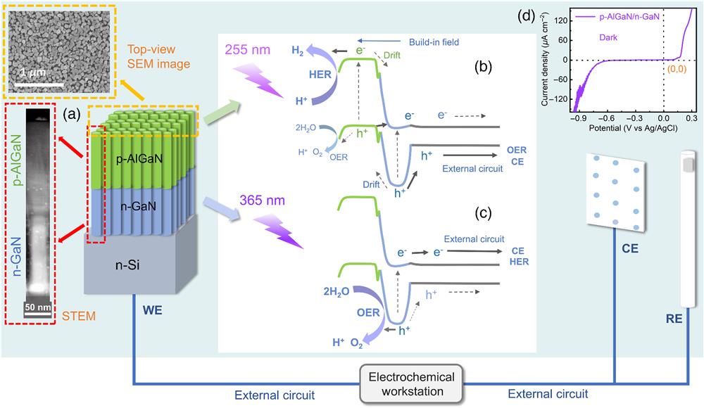
Three architectural types of AlGaN-based NWs were spontaneously grown on the n-type Si substrate by plasma-assisted molecular beam epitaxy (MBE) (see Sec. 4 for more details),36 including 160 nm bare p-AlGaN, 160 nm p-AlGaN/20 nm n-GaN, and 160 nm p-AlGaN/140 nm n-GaN NWs, which are schematically illustrated in Figs. S1(a)–S1(c) in the Supplemental Material. The overview micromorphology of the 160 nm AlGaN NWs with 140 nm GaN is demonstrated by the top-view scanning electron microscopy (SEM) image in the upper left inset of Fig. 1(a). In particular, the detailed feature of the single 160 nm p-AlGaN/140 nm n-GaN NW was zoomed in for characterization by scanning transmission electron microscopy (STEM) in the far left inset of Fig. 1(a). The surface morphologies of the other two AlGaN NW specimens were also characterized by SEM, which were displayed in Figs. S2(a) and S2(b) in the Supplemental Material. In addition, the 160 nm p-AlGaN/20 nm n-GaN NW specimen was also observed by STEM, as shown in Fig. S2(c) in the Supplemental Material. It can be seen from the SEM images that the three types of NWs have equal density distribution in morphology and are almost the same in average diameters.

Figure 1.(a) The schematic structure of the 160 nm p-AlGaN/140 nm n-GaN NWs. The far left inset is the STEM image of an individual NW, and the upper left inset is the top-view SEM image of the NWs. Operation mechanisms of the PEC PD under (b) 255 nm and (c) 365 nm illuminations, including energy band diagrams, carrier transport, and chemical reactions. The solid arrows refer to the dominant charge transfer processes. (d) The LSV curve of the PEC PD with 160 nm p-AlGaN/140 nm n-GaN NWs at dark.
The photoelectric characteristics of the PDs are monitored through the electrochemical workstation. To verify the influence of NW constitutions on the response of PDs, the photocurrent–time () responses under 365 and 255 nm lights are provided, respectively. As shown in Fig. 2(a), it can be noted that the constructed PEC PDs obtain a significant photocurrent without bias voltage, denoting the self-powered functionality of this PD. In Figs. 2(a) and 2(b), when the NW is illuminated by the 255 nm light, the workstation exhibits a large negative photocurrent signal; whereas, when the NW photoelectrode is exposed to 365 nm light, a positive photocurrent is recorded. In addition to the behavior of photocurrent polarity reversal depending on the light wavelength, both under 255 and 365 nm irradiation, the thicker GaN layer, the greater photoresponse in the constructed PEC PDs, in which the 160 nm p-AlGaN/140 nm n-GaN sample possesses the largest photocurrent in the three PD devices.
Figure 2.Photocurrent densities of the three constructed 160 nm p-AlGaN-based PEC PDs with 0, 20, and 140 nm n-GaN segments (namely, bare p-AlGaN, p-AlGaN/n-GaN-20 nm, and p-AlGaN/n-GaN-140 nm) under (a) 255 nm and (b) 365 nm illuminations. The response time () and recovery time () of the PDs with (c) 160 nm p-AlGaN/20 nm n-GaN and (d) 160 nm p-AlGaN/140 nm n-GaN NWs.
2.2 Working Principles of the PEC PD Based on p-AlGaN/n-GaN/n-Si Hybrid Dimension Platforms
As mentioned above, the NW heterojunction PEC PDs in this work can be modulated by changing the thickness of the GaN segment. To deeply reveal the underlying operating mechanism of the PEC PD with 160 nm p-AlGaN/140 nm n-GaN heterojunction, as illustrated in Figs. 1(a)–1(c), the simplified working principle schematic and corresponding energy band diagram under 255 and 365 nm illuminations are provided. (The achieved energy band diagrams of p-AlGaN/n-GaN were assisted by Silvaco TCAD. More details can be seen in Sec. 4.) In principle, when the n- and p-type semiconductors are in contact, electrons () in the n-GaN diffuse to the p-AlGaN, forming a built-in electric field directing from the GaN to the AlGaN. Meanwhile,when the NW contacts the electrolyte, an electrochemical equilibrium is established at the interface between the NW and electrolyte.37,38 As a result, an upward (downward) band bending would be manifested at the n-type (p-type) semiconductor/electrolyte interface on account of charge diffusion.37
As shown in Fig. 1(d), the current, derived from linear sweep voltammetry (LSV) measurement, increases very swiftly from a very small positive voltage bias (about 0.05 V) supplied by the workstation (reverse bias for p–n junction), which is attributed to the behavior of the carrier tunneling as the p–n band-edge alignment becomes more severely staggered under reverse bias. When the photoelectrode is applied under negative voltage bias (forward bias for p–n junction), the obvious current-rising occurs at a higher voltage (about ) compared to the threshold of tunneling. The current is categorized as diffusion current, which requires more negative bias (more forward bias for p–n junction), to balance out the barrier potential of the p–n junction to enhance the possibility of giving rise to the diffusion current. The obtained results from LSV measurement are in accordance with the characteristics of the p–n junction with a type-II band structure. More details are illustrated in Figs. S3(a)–S3(d) in the Supplemental Material.
When the NWs are exposed to the 365 nm light, only GaN segments respond to yield photogenerated carriers. Since the conduction band position of GaN is close to that of the Si substrate, the electrons can easily transport to the Pt CE through the Si platform.39,40 Meanwhile, due to the valence band offset between GaN and Si, parts of the photogenerated holes () from the GaN segment move toward the Si substrate. At the same time, many photogenerated holes migrate to the NWs/electrolyte interface to participate in the oxygen evolution reaction (OER) process under the combined action of upward surface band bending and the built-in field, thus exhibiting a forward photocurrent. Shown in Fig. 2(b), in contrast to the 160 nm bare AlGaN sample, the two samples with thicker GaN segment exhibit relatively obvious positive photocurrents.
When the light source switches to 255 nm, both AlGaN and GaN segments simultaneously absorb photons to produce electron–hole pairs. Under the built-in field of the p–n junction, some of the photogenerated electrons (holes) from the p-AlGaN (n-GaN) drift toward each other. However, thanks to the rather large contact area between AlGaN and electrolyte, most of the photogenerated electrons transfer to the AlGaN/electrolyte interface under the driving of downward surface band bending. Subsequently, the photogenerated electrons participate in the hydrogen evolution reduction (HER) reaction at the interface: ,10 whereas the photogenerated holes from the p-AlGaN move to the interface of the p–n junction to recombine with the electrons produced by the n-GaN NWs segment.35 Meanwhile, the excess photogenerated holes by the GaN segment migrate to the Pt CE through the external circuit and participate in the water oxidation reaction: .10 Then the ions diffuse to the WE through the electrolyte to undergo the reduction reaction. This cycling process of light trapping, carrier transport, and ion diffusion is realized without external bias and constitutes a complete circuit loop. Actually, an OER also exists on the AlGaN surface, but due to the downward band bending of p-AlGaN, it severely blocks the movement of photogenerated holes to the AlGaN/electrolyte interface, making the extremely weak OER activity negligible compared to HER. Thus the negative photocurrent is exhibited at 255 nm illumination, which forms the spectrally distinguishable self-sufficient PEC UV PD based on the p-AlGaN/n-GaN heterojunction NWs.
2.3 Dynamic Tuning Properties of the PEC PD with the GaN Thickness and External Input Changing
Here the net photocurrent density () is defined as , where is the current density with illumination, and is the current density at dark, respectively.41 And the net photocurrent density at 365 nm light (-365) increased from to when the GaN thickness varied from 20 to 140 nm (no obvious photocurrent can be perceived for the bare AlGaN NWs at 365 nm), which strongly implies that photoresponse behavior has a close relationship with the GaN segment. The improved positive photocurrent at 365 nm can be attributed to the more photogenerated carriers from 140 nm n-GaN NWs. Therefore, the number of electrons moving to the Si substrate increased, further boosting the positive photocurrent. Under 255 nm of illumination, it can be inferred that the net photocurrent densities () of the three samples are , , and , for the 160 nm p-AlGaN NW with 0, 20, and 140 nm GaN segments, respectively. When the NW with a longer GaN is illuminated at 255 nm light, more photogenerated electrons are generated from the GaN part than the other samples, causing more chances of recombination with the holes from the valence band of p-AlGaN by “Z” tunneling.35 It would, accordingly, induce a reduction in the recombination of photogenerated carriers from the p-AlGaN segment itself, thereby boosting the HER rate at the AlGaN/electrolyte interface.
In addition, the photoresponsivity is introduced to evaluate the device responsivity, namely, , where is the responsivity and is the incident light power, respectively.41 The responsivities of the constructed 160 nm p-AlGaN-based PD with 0, 20, and 140 nm GaN segments, are calculated as , (0.0028), and () under 255 nm (365 nm) illumination (0 V), respectively, which means that the GaN NWs play a pivotal role as the current flow “hub” at the p-AlGaN/n-GaN heterointerface for regulating the PD performance. These results demonstrate that the photoresponses can be adjusted by adopting different thicknesses of the GaN NWs under 255 and 365 nm lights, which expands the tunable range of high-response PEC devices.
In short, the GaN NW layers play different roles for different spectral responses: only acting as a photoabsorber at 365 nm light, while, under 255 nm illumination, primarily acting as an electron-donating layer to consume the holes generated from the AlGaN segment. When a whole heterojunction NW is under photoexcitation, the GaN segment is a crucial hub for regulating the carrier flow between the AlGaN segment and Si substrate, which is also evidenced by the photoresponse speed of the device. To reveal photoresponse speed under 255 nm irradiation, the response time and recovery time interval of the photocurrent are charted in Figs. 2(c) and 2(d). The is the time required for the photocurrent increasing from 10% to 90% of the maximum value, and the is the time taken by the photocurrent recovering from 90% to 10%. The corresponding and for the 160 nm p-AlGaN/140 nm n-GaN NWs are 50 and 100 ms, respectively. The photoresponse speed of this device is significantly improved compared to the 160 nm p-AlGaN/20 nm n-GaN NW, and and are 0.8 and 0.6 s, respectively.
Additionally, to testify the tunability of the device for complex applications in sophisticated environments, the photoresponse behaviors were recorded by changing incident light intensity or external bias [Fig. 3 and Fig. S4 in the Supplemental Material]. As illustrated in Figs. 3(a) and 3(b), both under 255 and 365 nm illuminations, the photocurrent density generally increases with increasing light intensity at 0 V. Moreover, due to the effects of electrostatic attraction from external bias, the generated electrons and holes are expedited to be separated. Thus, as indicated in Figs. 3(c) and 3(d), the negative current also increases with the increase of negative bias. To better illustrate the photocurrent changing by external bias, the LSV curve under 365 nm is adopted in Fig. 3(d). These results mean that the magnitude of the photocurrent can be flexibly manipulated by tuning illumination intensity and bias voltage.
Figure 3.PEC measurements of the constructed PEC PD with 160 nm p-AlGaN/140 nm n-GaN NWs. Photoresponses under (a) 255 nm and (b) 365 nm illuminations with various light intensities (0 V). (c) Photocurrents of the PEC PD under different biases (255 nm light). (d) LSV curve with a 30-s sampling interval under 365 nm illumination.
2.4 Pt-modified Surface Dynamics for High-Performance PEC UV Detector
Subsequently, to further improve the photoresponse of the constructed PEC PD with 160 nm p-AlGaN/140 nm n-GaN NWs, Pt modification was applied to promote the interfacial carrier dynamics on separation and transportation. As shown in Fig. 4, transmission electron microscopy (TEM) images of the 160 nm p-AlGaN/140 nm n-GaN NWs with Pt modification are provided, which are vertically aligned on the n-type Si wafer [Fig. 4(b)]. It can be seen in Figs. 4(c) and 4(d) that the dispersed Pt nanoparticles, with 2 to 6 nm diameters, are successfully deposited on the surface of the NWs. As illustrated in Fig. 5(a), after Pt decoration, the negative photocurrent density and responsivity, illuminated by 255 nm light, improved to and , respectively. As mentioned before, the photoresponse behaviors of the Pt-modified device can be adjusted by changing the light intensity and bias voltage as well [Figs. 5(a) and 5(b)], in which the photoresponsivity increased to at bias (255 nm light with ). In addition, as indicated in Fig. 5(c), the response time further decreases to 20 ms compared to the samples without Pt decoration mentioned above in this work. Comparing the trends of responsivity changes depending on the light intensity between before and after Pt decoration, it is remarkable that the responsivity drops down at high incident optical power for the NW without Pt, which is highlighted in Fig. 5(d). Actually, when the NWs without Pt are excited by high light intensity (e.g., ), a large number of photogenerated carriers would be hardly transferred into the external circuit loop simultaneously, which induces massive occurrence of carrier recombination within the p–n junction. Consequently, the photocurrent declines gradually over time in Fig. 5(e). On the contrary, due to the surface dynamic improvement, the phenomenon of recombination is suppressed within NWs and then the photocurrent attenuation can be alleviated prominently by Pt deposition on the AlGaN.
Figure 4.(a) Schematic structure of the 160 nm p-AlGaN/140 nm n-GaN NWs with Pt decoration grown on the Si substrate. (b), (c) Overview of the STEM images of the Pt/160 nm p-AlGaN/140 nm n-GaN NWs. (d) The energy-dispersive spectroscopy (EDS) elemental mapping images of the Pt/AlGaN/GaN structure.
Figure 5.Photoresponses of the PD with Pt/160 nm p-AlGaN/140 nm n-GaN NWs under (a) various irradiation intensities and (b) different biases. (c) Response time and recovery time of the PEC PD with Pt modification at 255 nm illumination. (d), (e) Responses comparison of the PEC PD with 160 nm p-AlGaN/140 nm n-GaN with and without Pt decoration. (f) Comparison of EIS curves at dark in these constructed PEC PDs.
Due to the inherent selectivity of photochemical deposition, Pt nanoparticles are preferentially anchored on the p-AlGaN surface sites.42,43 The Schottky junctions are formed between the AlGaN and Pt nanoparticles, boosting more electrons transferring from AlGaN to the Pt nanoparticles.44,45 The Pt modification facilitates the carrier separation and inhibits the recombination of the electron–hole pairs; therefore, the PEC signal is improved. For another thing, in metal nanoparticles, the collective oscillation of free electrons will induce localized surface plasmon resonance.44,46 Under UV light illumination, the Pt nanoparticles can enhance the scattering of the incident light, thereby contributing to the incident light absorption and more photogenerated carriers.47,48 Finally, and most importantly, Pt has excellent hydrogen adsorption energy, which mainly contributes to the HER process at the AlGaN/electrolyte interface, thus increasing the negative photocurrent.14,35,49 However, it has little impact on the positive photocurrent of 365 nm illumination [Fig. S5(a) in the Supplemental Material].
We also performed electrochemical impedance spectroscopy (EIS) measurements of the constructed PEC PDs [Fig. 5(f) and Fig. S5(b) in the Supplemental Material]. It is widely recognized that the diameter of the Nyquist plot is a vital indicator of the interface charge transfer resistance () characteristic between electrode and electrolyte.50,51 Apparently, the radius of the 160 nm p-AlGaN/140 nm n-GaN sample is smaller compared to that of 160 nm p-AlGaN/20 nm n-GaN, denoting that its transfer resistance is smaller, which is beneficial to carrier transport. Moreover, the transfer resistance is further reduced after decorating the NWs with Pt nanoparticles, which confirmed that the strategy of Pt modification indeed enhances the charge separation and transport, contributing to a larger photocurrent. The comparison of the responsivities with other previously reported dual-spectrum PDs is given in Table 1, which manifests that our constructed PEC PD is expected to be one of the optoelectronic devices with the most potential. Eventually, the long-term measurements with a 20-s sampling interval were carried out, suggesting that the detectors have good stability and repeatability [Fig. 6(a)]. After 1500 s, it can be observed that the photocurrent shows a slight decrease, which may be caused by the cracked NWs/substrate interface or the NWs being corroded in the solution for a long time. In addition, it was found that the photocurrent was reduced by 10% after 2 months, as shown in Fig. 6(b), indicating that the PD has the potential for practical application. In principle, some oxide films may be considered, such as , , and protective layers,52–54 to prevent the influence of long-term immersion of NWs, suppressing the current leakage.12,55 In addition, due to the upward surface band bending of GaN during PEC operation, most of the photoexcited holes would accumulate on the NW surface, which may lead to a photocorrosion effect.56,57 Future research may focus on embedding catalysts on the side of the GaN segment, which not only helps drive photoexcited holes to reaction sites to participate in redox reactions but also avoids photocorrosion, thereby intentionally improving device stability and photoresponsivity.
| Sample | Type | Source light (nm) | Photocurrent magnitude | Responsivity () | Reference |
| p-AlGaN/n-GaN (160 nm/140 nm) | PEC PD | 255 | | | This work |
| 365 | | 0.3 |
| Pt/p-AlGaN/n-GaN (160 nm/140 nm) | PEC PD | 255 | | | This work |
| 365 | | 0.36 |
| Solid-state PD | 254 | | 28.44 | 25 |
| 365 | | |
| Solid-state PD | 254 | | 43.9 | 26 |
| 365 | | |
| Solid-state PD | 254 | | 0.157 | 27 |
| 365 | | |
| ZnO/ZnS | Solid-state PD | 365 | | | 28 |
| 690 | | 0.364 |
| Solid-state PD | 400 | | | 29 |
| 800 | | 0.0145 |
| PEC PD | 254 | | 0.42 | 30 |
| 365 | | |
| PEC PD | 400 | | | 31 |
| 800 | | 0.15 |
| AlGaN/Pt-GaN cell | PEC PD | 254 | | 11.39 | 32 |
| 365 | | |
| Pt/GaN | PEC PD | 285 | | | 33 |
| 365 | | 1.1 |
| PEC PD | 254 | | | 34 |
| 365 | | 29.5 |
Table 1. Performance comparison between our constructed PDs and other recently reported PDs.
Figure 6.(a), (b) Long-time on/off cyclic photocurrent measurements of 160 nm p-AlGaN/140 nm n-GaN nanostructures under 255 nm illumination with an irradiation intensity of .
3 Conclusion
We systematically demonstrated the transport properties of p-AlGaN/n-GaN NWs self-powered PEC photodetection system, in which the significance of the GaN segment was fully elaborated. Compared to the bare AlGaN NW, the AlGaN/GaN NW PEC PD achieves photocurrent polarity reversal at two different light wavelengths and hence realizes spectrum distinguishing. When the NWs are excited by 365 nm light, the GaN just acts as a photoabsorber. While, under 255 nm illumination, the GaN primarily acts as an electron-donating layer to consume the holes generated from AlGaN segments, suppressing the carrier recombination within the AlGaN NWs, thus contributing to more electrons participating in the HER. In addition to changing the thickness of the GaN segment, the photoresponse of the NW PEC PD can be easily regulated by the light intensity and external bias, making it sensitive to the changes of ambient environment. Combining it with Pt decoration on AlGaN, the photoresponse performance can be further improved. This work verifies the feasibility of constructing high-performance PEC PD based on AlGaN/GaN NWs. Furthermore, on account of the photoresponse improvement together with precisely manipulating the structural constructions and the surface dynamics, a great model is established for synergistically optimizing structural designs of PEC PD by multiple strategies.
4 Detailed Methods
4.1 Growth of AlGaN Nanowires
P-AlGaN/n-GaN NWs with different lengths were grown on the n-type Si substrates via radio-frequency plasma-assisted MBE under nitrogen-rich conditions, which can reduce the formation of nitrogen-vacancy-related defects. The p-AlGaN segment can be grown by doping Mg at 390°C. To remove organic contaminants, the Si substrate was cleaned with acetone and methanol solvent. Subsequently, the native oxide on the Si wafer was removed by 10% hydrofluoric (HF) acid before loading into the MBE chamber. Herein, it is notable that when the 160 nm bare AlGaN NW sample was grown on the Si substrates, an ultrathin (~1 nm) GaN segment layer was introduced to obtain NWs with a better arrangement. The ultrathin GaN nucleating layer is rather deficient in light absorption efficiency. Thus in this sample, the GaN nucleating layer could be ignored and the NWs are considered as the bare AlGaN structure without GaN segment.
4.2 Characterization of the Electrodes
The microscopic morphology, crystal structure, and elemental composition of the samples were characterized by SEM, STEM, and EDS, respectively.
4.3 Pt Nanoparticle Photodeposition
The AlGaN NWs wafer was cut to the desired size and immersed with acetone, ethanol, and deionized water for 30 min, respectively. The pristine NWs were immersed into a precursor solution containing , 2 mL methanol, and 8 mL deionized water, and thereafter photodeposited under UV light for 15 min. Since the energy of the photogenerated electron was greater than the reduction potential of in the solution, resulting in the ions being reduced to Pt nanoparticles on the surface of the NWs, where abundant electrons exist. Then the NWs with co-catalyst were immersed into acetone and deionized water in turn and dried with an gas flow.
4.4 Semiconductor Simulation
Silvaco TCAD based on the ATLAS device simulator was adopted to analyze the energy band structure of p-AlGaN/n-GaN heterojunction NWs. Poisson’s equation and the continuity equation were used in the numerical procedures. For nitride semiconductors, polarization effects must be considered. The spontaneous and piezoelectric polarization effects were both taken into account for the polarization physical model.
4.5 Photoelectrode Fabrication
Both the pristine and Pt-decorated p-AlGaN/n-GaN NWs were encapsulated as follows to obtain photoelectrodes. First, the surface layer on the back side of the Si substrate was removed with a diamond pen. Then an ohmic contact was formed by coating a layer of In–Ga eutectic alloy on the Si surface. A copper sheet was subsequently connected to the In–Ga alloy area with silver paste. Finally, the entire photoelectrode was covered by utilizing insulating epoxy resin (except for the NW surface and part of the copper sheet) to prevent the electrolyte from connecting with the conducting Cu contact and leakage of the side or back of the Si substrate. The electrode should be dried for 24 h at room temperature before PEC measurements are carried out on the electrochemical workstation.
4.6 PEC Measurements
In this work, the 0.5 M aqueous solution was utilized as the electrolyte. Ag/AgCl (immersed in the saturated KCl solution) and Pt mesh were used as the RE and CE for photodetection, respectively. The p-AlGaN/n-GaN NW as the WE was performed in the standard three-electrode system electrochemical workstation (CHI 760E, Shanghai Chenhua). The PEC quartz reaction cell, which possesses high transmittance for UV light, was utilized. The switching of the light source is controlled by different wavelengths of LEDs (255 and 365 nm) together with a shutter (PFS40A), and the incident light power was calibrated by the UV light meter (LS125). The time-dependent photoresponse was measured at an interval of 0.001 s and a frequency of 20 s during the PEC tests. EIS measurements were performed in a frequency range from 0.1 to with 0.005 V amplitude.
Biographies of the authors are not available.
References
[1] D. Li et al. Solution grown single-unit-cell quantum wires affording self-powered solar-blind UV photodetectors with ultrahigh selectivity and sensitivity. J. Am. Chem. Soc., 141, 3480-3488(2019).
[2] U. Varshney, N. Aggarwal, G. Gupta. Current advances in solar-blind photodetection technology: using Ga2O3 and AlGaN. J. Mater. Chem. C, 10, 1573-1593(2022).
[3] S. Xu et al. Self-powered nanowire devices. Nat. Nanotechnol., 5, 366-373(2010).
[4] X. Liu et al. Power generation from ambient humidity using protein nanowires. Nature, 578, 550-554(2020).
[5] C. Soci et al. ZnO nanowire UV photodetectors with high internal gain. Nano Lett., 7, 1003-1009(2007).
[6] J. P. Zou et al. Ultraviolet photodetectors based on anodic TiO2 nanotube arrays. J. Phys. Chem. C, 114, 10725-10729(2010).
[7] Y. Wang et al. All-oxide NiO/Ga2O3 p–n junction for self-powered UV photodetector. ACS Appl. Electron. Mater., 2, 2032-2038(2020).
[8] X. Chen et al. Self-powered solar-blind photodetector with fast response based on Au/β-Ga2O3 nanowires array film Schottky junction. ACS Appl. Mater. Interfaces, 8, 4185-4191(2016).
[9] W. Jin et al. Self-powered high performance photodetectors based on CdSe nanobelt/graphene Schottky junctions. J. Mater. Chem., 22, 2863-2867(2012).
[10] J. Zhou et al. An overview on emerging photoelectrochemical self-powered ultraviolet photodetectors. Nanoscale, 8, 50-73(2016).
[11] X. Li et al. Nanocrystalline TiO2 film based photoelectrochemical cell as self-powered UV-photodetector. Nano Energy, 1, 640-645(2012).
[12] M. Jiang et al. Self-powered photoelectrochemical (Al, Ga)N photodetector with an ultrahigh ultraviolet/visible reject ratio and a quasi-invisible functionality for 360° omnidirectional detection. ACS Photonics, 8, 3282-3290(2021).
[13] D. Wang et al. Highly uniform, self‐assembled AlGaN nanowires for self‐powered solar‐blind photodetector with fast‐response speed and high responsivity. Adv. Opt. Mater., 9, 2000893(2020).
[14] D. Wang et al. Pt/AlGaN nanoarchitecture: toward high responsivity, self-powered ultraviolet-sensitive photodetection. Nano Lett., 21, 120-129(2021).
[15] S. Fang et al. Tuning the charge transfer dynamics of the nanostructured GaN photoelectrodes for efficient photoelectrochemical detection in the ultraviolet band. Adv. Funct. Mater., 31, 2103007(2021).
[16] L. Chen et al. Low-temperature synthesis of tin dioxide hollow nanospheres and their potential applications in dye-sensitized solar cells and photoelectrochemical type self-powered ultraviolet photodetectors. J. Power Sources, 272, 886-894(2014).
[17] J. V. S. Krishna et al. Solution processed aligned ZnO nanowires as anti-reflection and electron transport layer in organic dye-sensitized solar cells. Opt. Mater., 95, 109243(2019).
[18] W. Tian et al. Self-powered nanoscale photodetectors. Small, 13, 1701848(2017).
[19] X. Ren et al. Enhanced photoresponse behavior of Au@Bi2Te3 based photoelectrochemical-type photodetector at solid-solid-liquid joint interface. Mater. Today Energy, 16, 100401(2020).
[20] K. Chen et al. Photoelectrochemical self-powered solar-blind photodetectors based on Ga2O3 nanorod array/electrolyte solid/liquid heterojunctions with a large separation interface of photogenerated carriers. ACS Appl. Nano Mater., 2, 6169-6177(2019).
[21] L. Huang et al. A simple, repeatable and highly stable self-powered solar-blind photoelectrochemical-type photodetector using amorphous Ga2O3 films grown on 3D carbon fiber paper. J. Mater. Chem. C, 9, 10354-10360(2021).
[22] S. Chu et al. Artificial photosynthesis on III-Nitride nanowire arrays. Semicond. Semimet., 97, 223-255(2017).
[23] B. Zhou et al. Gallium nitride nanowire as a linker of molybdenum sulfides and silicon for photoelectrocatalytic water splitting. Nat. Commun., 9, 3856(2018).
[24] B. Ouyang et al. Dual-polarity output response-based photoelectric devices, 100418(2021).
[25] P. Li et al. Construction of GaN/Ga2O3 p–n junction for an extremely high responsivity self-powered UV photodetector. J. Mater. Chem. C, 5, 10562-10570(2017).
[26] T. Chen et al. Self‐powered and spectrally distinctive nanoporous Ga2O3/GaN epitaxial heterojunction UV photodetectors. Adv. Photonics Res., 2, 2100049(2021).
[27] K. Arora et al. Spectrally selective and highly sensitive UV photodetection with UV‐A,C band specific polarity switching in silver plasmonic nanoparticle enhanced gallium oxide thin‐film. Adv. Opt. Mater., 8, 2000212(2020).
[28] B. Ouyang, K. Zhang, Y. Yang. Photocurrent polarity controlled by light wavelength in self-powered ZnO nanowires/SnS photodetector system. iScience, 1, 16-23(2018).
[29] B. Ouyang et al. Dual-polarity response in self-powered ZnO NWs/Sb2Se3 film heterojunction photodetector array for optical communication. Nano Energy, 68, 104312(2020).
[30] C. He et al. α-Ga2O3 nanorod array-Cu2O microsphere p–n junctions for self-powered spectrum-distinguishable photodetectors. ACS Appl. Nano Mater., 2, 4095-4103(2019).
[31] C. V. Hoang et al. Interplay of hot electrons from localized and propagating plasmons. Nat. Commun., 8, 771(2017).
[32] X. Liu et al. Photovoltage‐competing dynamics in photoelectrochemical devices: achieving self‐powered spectrally distinctive photodetection. Adv. Funct. Mater., 32, 2104515(2021).
[33] S. Fang et al. Balancing the photo‐induced carrier transport behavior at two semiconductor interfaces for dual‐polarity photodetection. Adv. Funct. Mater., 32, 2202524(2022).
[34] D. Wang et al. Observation of polarity-switchable photoconductivity in III-nitride/MoSx core-shell nanowires. Light Sci. Appl., 11, 227(2022).
[35] D. Wang et al. Bidirectional photocurrent in p–n heterojunction nanowires. Nat. Electron., 4, 645-652(2021).
[36] Y. Wu et al. Molecular beam epitaxy and characterization of AlGaN nanowire ultraviolet light emitting diodes on Al coated Si (001) substrate. J. Cryst. Growth, 507, 65-69(2019).
[37] M. G. Kibria et al. Tuning the surface Fermi level on p-type gallium nitride nanowires for efficient overall water splitting. Nat. Commun., 5, 3825(2014).
[38] M. R. Nellist et al. Semiconductor-electrocatalyst interfaces: theory, experiment, and applications in photoelectrochemical water splitting. Acc. Chem. Res., 49, 733-740(2016).
[39] S. Vanka et al. High efficiency Si photocathode protected by multifunctional GaN nanostructures. Nano Lett., 18, 6530-6537(2018).
[40] Y. Wang et al. An In0.42Ga0.58N tunnel junction nanowire photocathode monolithically integrated on a nonplanar Si wafer. Nano Energy, 57, 405-413(2019).
[41] Z. Xie et al. Ultrathin 2D nonlayered tellurium nanosheets: facile liquid-phase exfoliation, characterization, and photoresponse with high performance and enhanced stability. Adv. Funct. Mater., 28, 1705833(2018).
[42] K. Wenderich, G. Mul. Methods, mechanism, and applications of photodeposition in photocatalysis: a review. Chem. Rev., 116, 14587-14619(2016).
[43] T. Takata et al. Photocatalytic water splitting with a quantum efficiency of almost unity. Nature, 581, 411-414(2020).
[44] X. Zhang et al. Plasmonic photocatalysis. Rep. Prog. Phys., 76, 046401(2013).
[45] K. Song et al. Plasmonic hot hole-driven water splitting on Au nanoprisms/P-type GaN. ACS Energy Lett., 6, 1333-1339(2021).
[46] W. Hou, S. B. Cronin. A review of surface plasmon resonance-enhanced photocatalysis. Adv. Funct. Mater., 23, 1612-1619(2013).
[47] X. Chang et al. Enhanced ultraviolet absorption in diamond surface via localized surface plasmon resonance in palladium nanoparticles. Appl. Surf. Sci., 464, 455-457(2019).
[48] Y. Kang et al. Coupling plasmonic Pt nanoparticles with AlGaN nanostructures for enhanced broadband photoelectrochemical-detection applications. ACS Appl. Nano Mater., 4, 13938-13946(2021).
[49] S. Chen, T. Takata, K. Domen. Particulate photocatalysts for overall water splitting. Nat. Rev. Mater., 2, 17050(2017).
[50] P. Varadhan et al. Surface passivation of GaN nanowires for enhanced photoelectrochemical water-splitting. Nano Lett., 17, 1520-1528(2017).
[51] Y. C. Chen, P. H. Dong, Y. K. Hsu. Defective indium tin oxide forms an ohmic back contact to an n-type Cu2O photoanode to accelerate charge-transfer kinetics for enhanced low-bias photoelectrochemical water splitting. ACS Appl. Mater. Interfaces, 13, 38375-38383(2021).
[52] Y. W. Chen et al. Atomic layer-deposited tunnel oxide stabilizes silicon photoanodes for water oxidation. Nat. Mater., 10, 539-544(2011).
[53] S. Hu et al. Amorphous TiO2 coatings stabilize Si, GaAs, and GaP photoanodes for efficient water oxidation. Science, 344, 1005-1009(2014).
[54] H. Kim et al. Enhanced photoelectrochemical stability of GaN photoelectrodes by Al2O3 surface passivation layer. Opt. Express, 27, A206-A215(2019).
[55] J. Zhang et al. A self-powered transparent photodetector based on detached vertical (In, Ga)N nanowires with 360 degrees omnidirectional detection for underwater wireless optical communication. Nanomaterials, 11, 2959(2021).
[56] M. G. Kibria et al. Atomic-scale origin of long-term stability and high performance of p-GaN nanowire arrays for photocatalytic overall pure water splitting. Adv. Mater., 28, 8388-8397(2016).
[57] B. AlOtaibi et al. Highly stable photoelectrochemical water splitting and hydrogen generation using a double-band InGaN/GaN core/shell nanowire photoanode. Nano Lett., 13, 4356-4361(2013).