Photonic structures with topological edge states and resonance loops are both important in optical communication systems, but they are usually two separate structures. In order to obtain a photonic system combining properties from both, we design multiple-layer nested photonic topological structures. The nested topological loops not only have topological protection immune to structural disorder and defects, but also possess both the properties of unidirectional propagation and loop resonance. Through mode analysis and simulations, we find that the transport can form diverse circulation loops. Each loop has its own resonance frequencies and can be solely excited in the nested layered structure through choosing its resonance frequencies. As a result, this work shows great application prospects in the area of reconfigurable photonic circuits.
Controlling the photonic flow of light on demand is critical for the next generation of photonic integrated circuits to meet the ever-expanding information explosion for data processing, communication, and computing. Topological photonics has brought about revolutionary schemes for the design of photonic components that enable robust light transport by topological protection. Topological photonics is the analogical study of topological insulators from which the quantum Hall (QH) effect and quantum spin Hall (QSH) effect are introduced into photonic systems[1–16]. Topological photonics provides a solid foundation to efficiently guide, switch, and route light in integrated circuits. But, only if the topological protection is combined with reconfigurability can it meet the request for the next generation of integrated devices. The ordinary topological transport exists only at the static structure boundary so that most of the footprint of the photonic structure is wasted. The reconfigurability of topological photonic transport pathways has been demonstrated in different structure systems and becomes a research hotspot[6–10]. For example, a photonic topological insulator (PTI) with mechanical reconfigurability was demonstrated in the gigahertz (GHz) region[11]. Another dynamically reconfigurable topological edge state is achieved in phase change photonic crystals (PCs)[10]. In Ref. [8], the non-Hermitian-controlled topological state enables the dynamic control of robust transmission links of light inside the bulk. Very recently, the topological photonic modes have been switched on or off through changing the liquid crystal orientation[9] and the effective refractive index of the grating[10]. The above-mentioned reconfigurability has to rely on the external conditions, such as the mechanical force, to change the configuration of scatterers[6], the voltage to modulate material refractive index[7], and the pumping energy to induce the local non-Hermitian symmetry breaking[8]. These external conditions can dynamically change the topological transport pathways.
In this work, we propose a different reconfigurability scheme of photonic topological transport pathways. We design multilayer nested photonic topological loops similar to a Russian doll. Through the tuning of light frequency, the transport channels in the structures can take on interesting and diverse forms, such as single external loop, single inner loop, and single middle loop. Compared with the other similar schemes, the unique value of our designed structure is that the reconfigurability of the topological loop channels does not need any external condition, and it can be achieved through the signal source frequency, which greatly reduces the difficulty and complexity of the design.
2. Topological Edge States and Loop Models
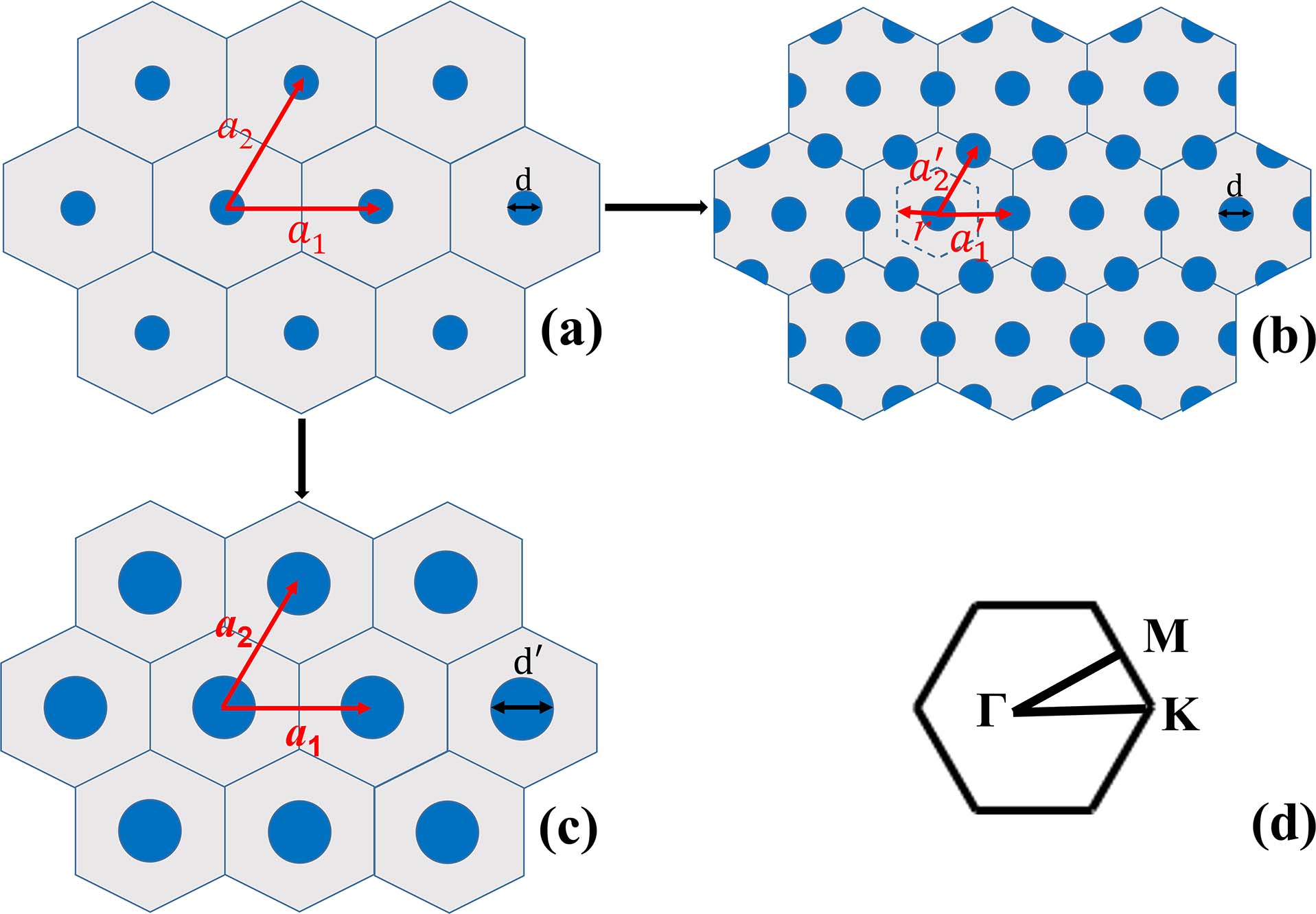
The design begins with a two-dimensional (2D) PC made of purely dielectric rods in a triangular lattice, as shown in Fig. 1(a). In Fig. 1(a), and are the lattice basic vectors, where is the lattice constant. The rods have the permittivity of 11.7 and the diameter of . The background is the air. The first Brillouin zone with three highly symmetric points is shown in Fig. 1(d). The hexagon is the lattice primitive cell (the smallest structure period). We call such a structure the A-lattice. Later we shrink A-lattice to that in Fig. 1(b), in which we choose the lattice basic vectors as and , and the lattice constant becomes . We call the lattice in Fig. 1(b) the B-lattice. If we set a boundary between the two lattices A and B and calculate the edge states, we have to take the smallest common period of the two lattices. The smallest common period is just the solid hexagonal in Figs. 1(a) and 1(b), respectively. Thus, for the later study of edge states, the eigenfrequency calculations must use the solid hexagonal as the unit cell for both the lattices. In the calculations performed by COMSOL Multiphysics, the TM modes of the electromagnetic wave (the fields with , , and components) are considered. In order to obtain the common band gaps of A-lattice and B-lattice, we enlarge the rod diameter of A-lattice to . Thus, A-lattice becomes C-lattice. The frequency bands for C-lattice and B-lattice are shown in Figs. 2(a) and 2(b) with the direction in the first Brillouin zone. The triangular lattice has a point group symmetry. The eigenstates at point have two irreducible representations: and . As shown in Fig. 2(a), the mode fields of the two degenerate points are similar to the -orbit and -orbit of the electron wave function in quantum mechanics[11], respectively. corresponds to the dipole state with double degeneration, i.e., two -orbits, and , with odd parity; corresponds to the quadrupole state with double degeneration, i.e., two -orbits, and , with even parity. For A-lattice, the frequency of -orbit is higher than that of -orbit, and the corresponding band gap is topologically trivial. For B-lattice, because we have used the enlarged unit cell, a band fold occurs, leading to the frequency bands in Fig. 2(b). Because of the band fold, two pairs of bands are also degenerated. Different from the orbit positions in Fig. 2(a), the frequency of -orbit is smaller than that of -orbit in Fig. 2(b), i.e., the two orbits have been reversed, and the corresponding bandgap is topologically nontrivial.
Sign up for Chinese Optics Letters TOC. Get the latest issue of Chinese Optics Letters delivered right to you!Sign up now
Figure 1.Schematic of triangular lattice in different forms. (a) A-lattice. The primitive cell consisting of one dielectric rod with the permittivity of 11.7, a1 and a2 are unit vectors with the length of a as the lattice constant, and d = 0.32a is the rod diameter. (b) B-lattice. The rods are the same as those in A-lattice. a1′ and a2′ are the unit vectors with length a/2. The solid hexagonals are the unit cell including one rod and six semi-rods in the unit cell. (c) C-lattice. The lattice is the same as A-lattice, but the primitive cell consists of one dielectric rod with the diameter d = 0.578a. (d) The first Brillouin zone with the unit vectors a1 and a2.
Figure 2.Eigenfrequency bands of (a) C-lattice and (b) B-lattice. (c) The p-orbit and d-orbit reversal process with the value of r. It is clear that the d-orbit position has a sharp drop, and it occurs because the dashed unit cell is tangent to rods. The gray region is the common bandgap.
In order to show the evolution of topological phase from A-lattice to B-lattice, based on B-lattice, we further choose a dashed hexagon with the distance from the center to the side of the dashed hexagon. The value of is increased from to . The new unit cell with only corresponds to B-lattice.
We use the dashed hexagon as the new unit cell to perform the frequency band calculation and record the positions of -orbit and -orbit with increasing from to . The result is shown in Fig. 2(c), in which the evolution of the two orbits clearly shows the process of orbit reversal. It is clear that the -orbit position has a sharp drop, and it occurs because the dashed unit cell is tangent to rods.
The key to realize the QSH effect in optical systems is to build the optical pseudospin states. The effective Hamiltonian of the system is expressed as[14]where is the effective Hamiltonian at . and are the eigenfrequencies of and orbits, respectively. is a perturbation term, which can be expressed as where is the overlapping integral between different basic vectors and . Through the transformation of basic vectors, under the new basic vector space, the effective Hamiltonian is rewritten as with , where , is the non-diagonal term of the first-order perturbation , and comes from the diagonal term of the second-order perturbation , which is a negative value. Then, the spin Chern number can be simplified as
The results of Eq. (4) are based on the values of . leads to corresponding to the topologically nontrivial state, whereas leads to corresponding to the topologically trivial state. For a normal case, , , and . For the reversal case, , , and . Therefore, the band reversal will lead to the topology transition.
Furthermore, B-lattice and C-lattice have a large common bandgap from 0.44() to 0.548(). Such a large common bandgap can warrant an intense localization effect of edge states. The intense localization effect is in favor of the formation of multiple-layer dense circulation loops. There is an extra band (black solid line) between and -orbit. The formation of the extra band is accidental because when the rod diameter of A-lattice increases, the band below -orbit slowly moves up and passes over the -orbit, resulting in the inserted band. But, the inserted band only decreases the width of the nontrivial band gap and does not affect the topological properties of nontrivial band gap, just as the inserted band in Ref. [17].
According to the bulk-boundary correspondence, the topological edge states should exist at the interface between trivial and nontrivial systems, analogous to the QSH effect in electronics. To find and study the edge states, a supercell including the interface of lattices B and C has to be constructed, which is denoted by the rectangle in Fig. 3(b). In order to enhance the localization effect of edge states, we construct a compound boundary configuration by enlarging the interval between the trivial and nontrivial PCs. This configuration will realize the coupling of topological edge states and the line defect states. At the interface, the distance between two rods from lattices B and C has been optimized to . The supercell has the smallest common period in the truncated () direction for the two lattices and is infinite in the direction, but we have to take a finite length in the direction in real calculations. The frequency bands for the supercell are given in Fig. 3(a). There is only one symmetric edge state curve inside the large bandgap. The large bandgap of the supercell is due to the large common bandgap of B-lattice and C-lattice. The time-averaged Poynting vectors for two symmetric points P and Q on the curve are shown in Fig. 3(b). It is found that there is one energy flow vortex within the edge rod of C-lattice for both points P and Q, and a parallel energy flow within the gap of the two lattices. The two kinds of energy flows mean that the modes P and Q are the hybrid results of the ordinary line defect state and topological edge state. The hybrid edge state is due to the large space gap between the two lattices. The ordinary topological edge state curves are usually a pair of two symmetric curves that almost extend to the whole bandgap range. Only a mini-gap may occur in the edge modes due to the small mismatching of lattices. In this occasion, due to the large mismatching of lattices, the gap of the two curves is made so large that the other branch curve is pushed into the bulky band. The rotation directions for points P and Q are anticlockwise and clockwise, respectively. In fact, all the points on the left branch curve (right branch curve) have the same rotation direction as point P (point Q). The opposite energy flow vortices mean that the transport direction of the edge states may be spin-locked. If the source spin is clockwise (anticlockwise), the transport direction is locked to the group velocity direction of the right (left) curve branch, i.e., the direction. The similar topologically protected defect modes have been proposed in Refs. [18,19]. In Ref. [19], the authors propose a similar compound boundary configuration of the line air defect and the topological edge states. The topological line defect state can be excited to form unidirectional transmission locked by the pseudospin sources and is robust to the disorders. Chen et al.[19] have also considered the coupling between the edge states and the line defect state. But, in their paper, the compound boundary configuration is “the nontrivial PC-air-nontrivial PC”, while ours is “the nontrivial PC-air-trivial PC.”
Figure 3.(a) Edge state dispersion curve from the two lattices. The left curve branch and the right curve branch have the negative and positive group velocities, respectively. (b) The energy flow vectors around the edge corresponding to the edge states P and Q in (a).
To demonstrate the spin-locked unidirectional transport, we perform the frequency-domain simulations in a frequency range on the edge state curve. In our article, the design is excited by a point source with pseudospin at a specific frequency in the simulation model. The boundary conditions are set to be the scattering boundary condition. In order to excite the topological edge state from the hybrid state, the point source with pseudospin has to be placed close to the large rod at the edge of the C-lattice. Figures 4(a) and 4(b) are the results with the spin source of on the boundary. The frequency line has two interest points with the edge state curve. The anticlockwise source excites the mode on the left of the curve with negative group velocity, while the clockwise source excites the mode on the right of the curve with positive group velocity. In order to verify the property of the topological edge state, in Figs. 4(c) and 4(d), we show the transmission results of the spin source with in the topological edge state waveguide and the spin source with in the ordinary line defect waveguide with a bend (from the B-lattices), respectively. All of the field distributions are the amplitude of electric fields. The topological edge state in Fig. 4(c) has the performance of robustness against sharp bends, but the ordinary edge state in Fig. 4(d) is bidirectional and cannot pass the sharp bends. In the frequency range over the dashed line corresponding to in Fig. 3(a), all the simulations of the topological edge state waveguide and the spin source edge states show the property of unidirectional transport. Below , the spin-locked transport becomes invalid, and both the unidirectional transport and bidirectional transport will occur at different frequencies. The simulation results are in good agreement with the above theoretical analysis.
Figure 4.Edge state transport simulations. (a) The straight edge state with anticlockwise source. (b) The straight edge state with clockwise source. (c) The topological edge state with a sharp bend. (d) The ordinary edge state with a sharp bend.
The spin-locked unidirectional transport provides us with a space of designing diverse photonic loops. In Fig. 5, we give some models of nested photonic topological loops. The white regions are B-lattice (topologically nontrivial) and the gray regions are C-lattice (topologically trivial). There are some nested hexagons. Each hexagon is divided into two isosceles trapezoids. In the upper half-space, the isosceles trapezoids are denoted as , and, in the lower half-space, the isosceles trapezoids are denoted as in turn from inner to outer. The source is placed at the interface of the two lattices. The unidirectional transport can form photonic loops around these trapezoids with definite rotation direction. Figure 5 shows all potential transport paths denoted by the dashed arrows. The two solid arrows denote the input and the output light flows. For the clockwise spin source, if the inside and outside loops are C-lattice and B-lattice, respectively, the loop rotation direction is clockwise; conversely, if the inside and outside loops are B-lattice and C-lattice, respectively, the loop rotation direction is anticlockwise. On the other hand, for the anticlockwise spin source, the case is reversed. However, whether the potential transport paths can be realized is dependent on the source frequency or wavelength and the loop optical length, because in a closed loop the phase change can result in the constructive or destructive interference. For a loop length , the total phase change is equal to , in which ( is the group velocity of the edge state). If , the loop will lead to a constructive interference and form a resonator, while if ( is an integer number), the loop will lead to a destructive interference, and there is no transport in the loop. Therefore, for the fixed loops, through adjusting the source frequency, the reconfigurable diverse photonic topological loops can be achieved. The conventional photonic loops or cavities cannot be made as multiple layers with high density, and the transport paths in them are always fixed.
Figure 5.Model designs of nested topological loops. (a) One layer with clockwise spin source. (b) Two layers with anticlockwise spin source. The dashed arrows denote all the potential photonic paths. The white and gray regions are B-lattice (topologically nontrivial) and C-lattice (topologically trivial), respectively. The red and blue arrows denote the light flows along the loops A and B, respectively.
3. Simulations of Diverse Topological Photonic Loops
The unidirectional transport of the topological edge states provides the condition to form the photonic loops. According to Fig. 5, we construct the frequency-domain simulation models of nested topological loops from one layer to two layers. In order to account for the results, we define the loop around as , in which “” is the region forming the loop, “[ ]” denotes the loop around , and “+” (“-”) represents the clockwise (anticlockwise) rotation direction of loops. The other loops are denoted in the same way. Figure 6 shows the four different results of the one-layer loop for the same clockwise spin source with four frequencies. The side length of the loop is . In Fig. 6(a), the intense resonance field is along both the peripheries of and with reversed directions, but the field on the common side of and is too small to be seen in the 2D field plot. The small field on the common side is because at the common side the two light flows from and are not in phase, and the superposed fields quickly decrease compared with the other branches in and . Figure 6(b) is similar to Fig. 6(a), but, at the common side, the two light flows from and are in phase, and the superposed fields lead to a constructive interference. In both Figs. 6(a) and 6(b), the loops form the resonator because the input and output fields are much smaller than the resonance fields in the loops. In brevity, we define the loops of Figs. 6(a) and 6(b) as and , respectively. Figures 6(c) and 6(d) are similar to Figs. 6(a) and 6(b), respectively. The difference is that in Figs. 6(c) and 6(d) the input and output fields are close to the fields in the loops. Hence, there is no resonance enhancement in Figs. 6(c) and 6(d), and the loops have no resonance effect. To account for it, we plot the one-dimensional fields along the common side from Figs. 6(b) and 6(d) in Fig. 7. In Fig. 6(b), the field on the common side is much larger than the input and the output
Figure 6.Light flows from the clockwise spin source in a one-layer topological loop with normalized angular frequencies: (a) 0.53(2πc/a), (b) 0.5034(2πc/a), (c) 0.5348(2πc/a), and (d) 0.5504(2πc/a). The side length of loop is 9a.
Figure 7.One-dimensional fields along the line through the source and the common side in Fig. 6(b) with the resonance loop and in Fig. 6(d) with the non-resonance loop.
Next, we consider the case of two-layer topological loops shown in Fig. 5(b). The size of the inner layer is the same as that in Fig. 6. The outer loop has the side length . Through adjusting the frequency of the anticlockwise spin source, we obtain four typical results shown in Fig. 8. In Fig. 8(a) with () and in Fig. 8(b) with (), only the inner loops have been excited with the opposite rotation direction to that in Fig. 6, which are denoted as and , respectively. The frequencies are the same as those in Figs. 6(a) and 6(b), respectively. The resonance condition for the inner loop is the same as that in Fig. 6. Thus, even if the light first meets the outer loop, the resonance condition allows the light to break through the outer loop and excite the inner loop. In Fig. 8(c) with (), only the outer loop has been excited, which is denoted as . In Fig. 8(d) with (), all potential resonance loops have been excited, which are denoted as .
Figure 8.Light flows from the anticlockwise spin source in two-layer topological loops with normalized angular frequencies: (a) 0.53(2πc/a), (b) 0.5034(2πc/a), (c) 0.5227(2πc/a), and (d) 0.4991(2πc/a). The outer loop has the side length of 15a.
To summary, in Table 1, we write all potential forms of loops from one layer to two layers. In the table, the forms of loops with larger layer numbers include the forms of loops with smaller layer numbers. Although we have only displaced the results of the nested loops with two layers, the controllable transport loops can be extended to the nested structure with any number of layers.
Normalized Frequency
One Layer
Two Layers
0.5189/0.53
[A1+ + B1−]
[A1+ + B1−]
0.5034/0.5105
[A1+] + [B1−]
[A1+] + [B1−]
0.5227
[A2+ + B2−]
0.4991
[A1+] + [B1−] + [A2+] + [B2−]
Table 1. Forms of Nested Loops with Different Layer Numbers
In summary, we have designed the reconfigurable topological channels in the form of multiple-layer nested loops. Although the reconfigurable topological waveguides have been widely studied, the unique value of our design is that the reconfigurable method does not rely on the external conditions; instead, the selective excitation of different loops is dependent on the source frequency. Thus, we have provided a new reconfigurable method for topological waveguides. In its multiple applications, the potential application in laser resonators may be expected. For general laser resonators, the defect and disorder will affect the loss threshold of lasers and reduce the output power largely. If our current topological loops are used as the laser resonators, their ability to be immune to the defect and disorder will make the laser work with high output efficiency and more stability. Therefore, the new reconfigurable and diverse photonic loop channels combined with topological protection will find important applications in the design of a variety of photonic devices.
References
[1] L. Lu, J. Joannopoulos, M. Soljačić. Topological photonics. Nat. Photonics, 8, 821(2014).
[2] A. B. Khanikaev, G. Shvets. Two-dimensional topological photonics. Nat. Photonics, 11, 763(2017).
[3] T. Ozawa, H. M. Price, A. Amo, N. Goldman, M. Hafezi, L. Lu, M. C. Rechtsman, D. Schester, J. Simon, O. Zilberg, L. Carusotto. Topological photonics. Rev. Mod. Phys., 91, 015006(2019).
[4] B. Yan, J. Xie, E. Liu, Y. Peng, R. Ge, J. J. Liu, S. C. Wen. Topological edge state in the two-dimensional stampfli-triangle photonic crystals. Phys. Rev. Appl., 12, 044004(2019).
[5] X. C. Sun, C. He, X. P. Liu, M. H. Lu, S. N. Zhu, Y. F. Chen. Two-dimensional topological photonic systems. Prog. Quant. Electron., 55, 52(2017).
[6] X. J. Cheng, C. Jouvaud, X. Ni, S. H. Mousavi, A. Z. Genack, A. B. Khanikaev. Robust reconfigurable electromagnetic pathways within a photonic topological insulator. Nat. Mater., 15, 542(2016).
[7] T. Cao, L. H. Fang, Y. Cao, N. Li, Z. Y. Fan, Z. G. Tao. Dynamically reconfigurable topological edge state in phase change photonic crystals. Sci. Bull., 64, 814(2019).
[8] H. Zhao, X. D. Qiao, T. W. Wu, B. Midya, S. Longhi, L. Feng. Non-Hermitian topological light steering. Science, 365, 1163(2019).
[9] M. I. Shalaev, S. Desnavi, W. Walasik, N. M. Litchinitser. Reconfigurable topological photonic crystal. New J. Phys., 20, 023040(2018).
[10] C. Li, X. Y. Hu, W. Gao, Y. T. Ao, S. S. Chu, H. Yang, Q. H. Gong. Thermo-optical tunable ultracompact chip-integrated 1D photonic topological insulator. Adv. Opt. Mater., 6, 1701071(2018).
[11] L. H. Wu, X. Hu. Scheme for achieving a topological photonic crystal by using dielectric material. Phys. Rev. Lett., 114, 223901(2015).
[12] X. T. He, E. T. Liang, J. J. Yuan, H.-Y. Qiu, X.-D. Chen, F.-L. Zhao, J.-W. Dong. A silicon-on-insulator slab for topological valley transport. Nat Commun., 10, 872(2019).
[13] M. I. Shalaev, W. Walasik, A. Tsukernik, Y. Xu, N. M. Litchinitser. Robust topologically protected transport in photonic crystals at telecommunication wavelengths. Nature Nanotech., 14, 31(2019).
[14] Y. L. Wang, Y. Li. Pseudospin states and topological phase transitions in two-dimensional photonic crystals made of dielectric materials. Acta Phys. Sin., 69, 094206(2020).
[15] Z. Jiang, Y. F. Gao, L. He, J. P. Sun, H. Song, Q. Wang. Manipulation of pseudo-spin guiding and flat bands for topological edge states. Phys. Chem. Chem. Phys., 21, 11367(2019).
[16] S. Barik, H. Miyake, W. DeGottardi, E. Waks, M. Hafezi. Two-dimensionally confined topological edge states in photonic crystals. New J. Phys., 18, 113013(2016).
[17] Y. T. Fang, Z. X. Wang. Highly confined topological edge states from two simple triangular lattices with reversed materials. Opt. Commun., 479, 126451(2021).
[18] Y. F. Gao, Z. Jiang, S. Y. Liu, Q. L. Ma, J. P. Sun, H. Song, M. Zamani. Topologically protected defect modes in all-dielectric photonic crystals. J. Phys. D, 53, 365104(2020).
[19] M. L. Chen, L. J. Jiang, Z. Lan, W. Sha. Pseudospin-polarized topological line defects in dielectric photonic crystals. IEEE T Antenn Propag., 68, 609(2020).