• Photonics Research
  • Vol. 9, Issue 5, 734 (2021)
Jiaxing Wang1、2、†, Chunshuang Chu1、2、†, Kangkai Tian1、2, Jiamang Che1、2, Hua Shao1、2, Yonghui Zhang1、2, Ke Jiang3, Zi-Hui Zhang1、2、4、*, Xiaojuan Sun3、5、*, and Dabing Li3
Author Affiliations
  • 1State Key Laboratory of Reliability and Intelligence of Electrical Equipment, Hebei University of Technology, Tianjin 300401, China
  • 2Key Laboratory of Electronic Materials and Devices of Tianjin, School of Electronics and Information Engineering, Hebei University of Technology, Tianjin 300401, China
  • 3State Key Laboratory of Luminescence and Applications, Changchun Institute of Optics, Fine Mechanics and Physics, Chinese Academy of Sciences, Changchun 130033, China
  • 4e-mail: zh.zhang@hebut.edu.cn
  • 5e-mail: sunxj@ciomp.ac.cn
  • show less
    DOI: 10.1364/PRJ.418813 Cite this Article Set citation alerts
    Jiaxing Wang, Chunshuang Chu, Kangkai Tian, Jiamang Che, Hua Shao, Yonghui Zhang, Ke Jiang, Zi-Hui Zhang, Xiaojuan Sun, Dabing Li. Polarization assisted self-powered GaN-based UV photodetector with high responsivity[J]. Photonics Research, 2021, 9(5): 734 Copy Citation Text show less
    Schematic structures for (a) Device R and (b) Device N. (c) Top view of GaN-based MSM PD showing interdigital electrodes. Schematic energy band diagrams of (d) Device R and (e) Device N.
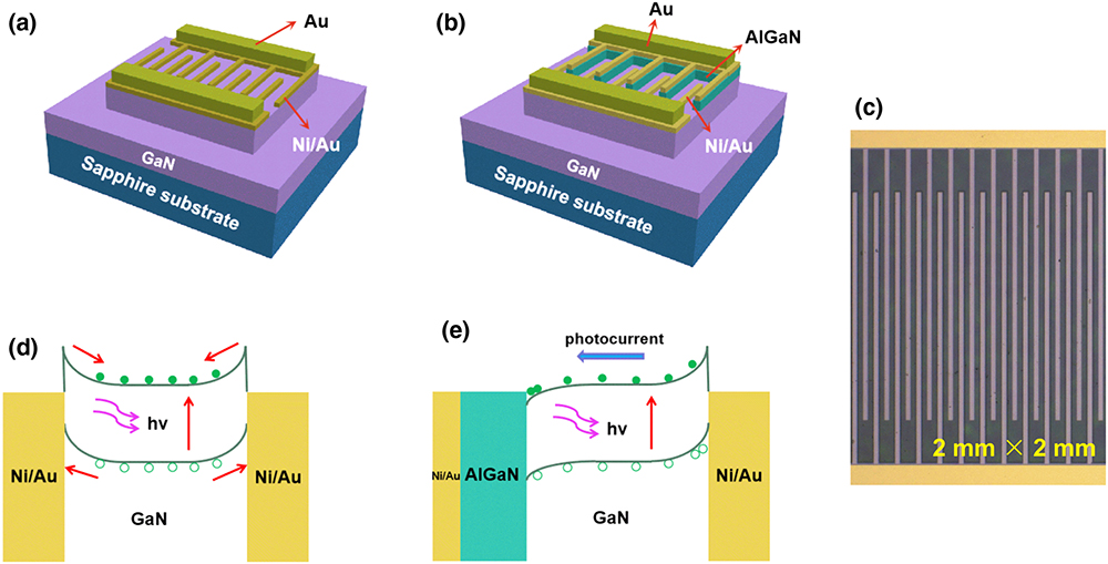
    Fig. 1. Schematic structures for (a) Device R and (b) Device N. (c) Top view of GaN-based MSM PD showing interdigital electrodes. Schematic energy band diagrams of (d) Device R and (e) Device N.
    (a) Dark current and photocurrent in terms of the applied bias for Devices R and N. Photocurrent for (b) Device R and (c) Device N in terms of different laser powers. (d) Two-dimensional electric field profiles and (e) current distributions for Devices R and N at the applied bias of 3 V under the 266 nm UV illumination. The bias is applied at the left electrode, such that the positive bias is biased at the left electrode in the first quadrant and the negative bias is biased at the left electrode in the second quadrant. The other electrode is grounded when the devices are measured. The wavelength for the illumination laser is 266 nm. The positive direction for the electric field is defined to point to the right side in (d).
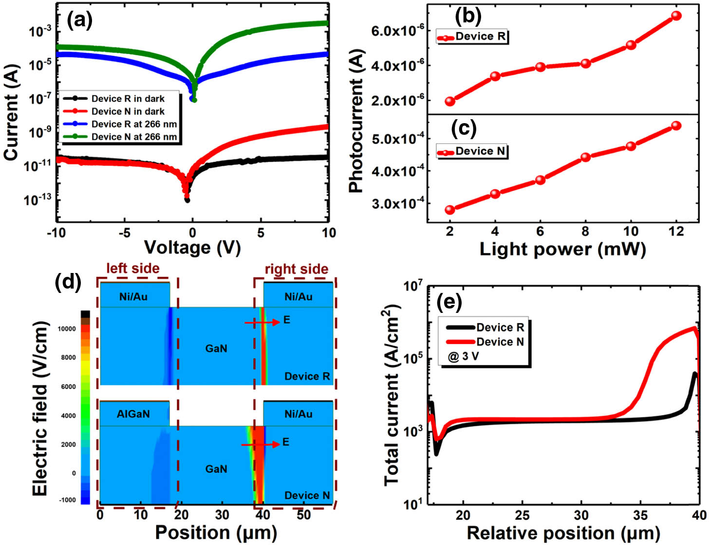
    Fig. 2. (a) Dark current and photocurrent in terms of the applied bias for Devices R and N. Photocurrent for (b) Device R and (c) Device N in terms of different laser powers. (d) Two-dimensional electric field profiles and (e) current distributions for Devices R and N at the applied bias of 3 V under the 266 nm UV illumination. The bias is applied at the left electrode, such that the positive bias is biased at the left electrode in the first quadrant and the negative bias is biased at the left electrode in the second quadrant. The other electrode is grounded when the devices are measured. The wavelength for the illumination laser is 266 nm. The positive direction for the electric field is defined to point to the right side in (d).
    (a) Spectral responsivity, (b) and (c) energy band diagrams near the GaN layer surface, and (d) two-dimensional electric field profiles for Devices R and N at the applied bias of 0 V under 266 nm UV illumination. Ec, Ev, Efe, and Efh denote energies of the conduction band, the valence band, and quasi-Fermi levels for electrons and holes, respectively. The positive direction for the electric field is defined to point to the right side in (d).
    Fig. 3. (a) Spectral responsivity, (b) and (c) energy band diagrams near the GaN layer surface, and (d) two-dimensional electric field profiles for Devices R and N at the applied bias of 0 V under 266 nm UV illumination. Ec, Ev, Efe, and Efh denote energies of the conduction band, the valence band, and quasi-Fermi levels for electrons and holes, respectively. The positive direction for the electric field is defined to point to the right side in (d).
    Spectral responsivity for (a) Device R and (b) Device N at different applied biases.
    Fig. 4. Spectral responsivity for (a) Device R and (b) Device N at different applied biases.
    Time-dependent photo-response characteristics for (a) Device R and (b) Device N when devices are biased to 3 V. The laser wavelength is 266 nm.
    Fig. 5. Time-dependent photo-response characteristics for (a) Device R and (b) Device N when devices are biased to 3 V. The laser wavelength is 266 nm.
    Wavelength (nm)Absorption Coefficient (m1)
    2503.355×107
    2603.140×107
    2702.927×107
    2802.714×107
    2902.500×107
    3002.283×107
    3102.058×107
    3201.823×107
    3301.570×107
    3401.287×107
    3509.459×106
    3604.189×106
    3701.704×105
    3806.500×103
    3902.933×102
    4001.545×101
    Table 1. Absorption Coefficient of GaN Under Different Wavelengths
    MaterialResponsivityWavelength (nm)Self-poweredOn/Off RatioYearRefs.
    GaN0.00154 A/W at 0 V340Yes2016[36]
    GaN3.096 A/W at 10 V360No1062017[16]
    Al0.6Ga0.4N/Al0.5Ga0.5N106  A/W at 5 V250No5×1062017[35]
    GaN0.28 A/W at 10 V325Yes<102018[37]
    AlGaN0.115 A/W at 0 V, 0.154 A/W at 3 V270Yes2018[38]
    GaN0.633 A/W at 5 V325Yes<102018[21]
    Al0.4Ga0.6N0.30 A/W at 8 V265No1062019[2]
    GaN0.147 A/W at 3 V368No1042019[39]
    Ultra-thin GaN0.00176 A/W at 0 V325Yes<102020[26]
    Al0.45Ga0.65N3.10 A/W at 30 V250No1042020[40]
    GaN0.005 A/W at 0 V, 13.56 A/W at 3 V346Yes1062021This work
    Table 2. Performances for the Reported GaN-Based and AlGaN-Based PDs in the Literature
    Jiaxing Wang, Chunshuang Chu, Kangkai Tian, Jiamang Che, Hua Shao, Yonghui Zhang, Ke Jiang, Zi-Hui Zhang, Xiaojuan Sun, Dabing Li. Polarization assisted self-powered GaN-based UV photodetector with high responsivity[J]. Photonics Research, 2021, 9(5): 734
    Download Citation