
Jiaxing Wang, Chunshuang Chu, Kangkai Tian, Jiamang Che, Hua Shao, Yonghui Zhang, Ke Jiang, Zi-Hui Zhang, Xiaojuan Sun, Dabing Li, "Polarization assisted self-powered GaN-based UV photodetector with high responsivity," Photonics Res. 9, 734 (2021)
- Photonics Research
- Vol. 9, Issue 5, 734 (2021)
Abstract
1. INTRODUCTION
Ultraviolet (UV) detection is an important technology in military and civil applications, such as missile warning, fire monitoring, public security investigation, and environmental detection [1–4]. To achieve UV detection, wide-band-gap semiconductors have to be used, and thus research efforts have been currently devoted to SiC, ZnO,
An effective method to increase the responsivity is making Schottky contacts with different metals for MSM PDs. Then the different work functions for the two metals will produce the asymmetric energy band, which is very useful to promote the carrier transport. Moreover, such asymmetric energy band profiles can even generate photocurrent when the devices are not biased, i.e., a self-powered MSM PD is achieved [21–25]. One typical AlGaN-based PD with an asymmetric structure is achieved by using Ni and Au as electrodes at the two ends; the different barrier heights for the Ni/GaN and Au/GaN junctions enable more efficient charge transport and the increased responsivity [22]. However, the responsivity can be further promoted if the energy band can be made more asymmetric. For that purpose, a Pt-Ag GaN MSM PD is reported. The very large potential gradient of 1.39 eV between the Pt and Ag metals then favors the enhanced thermionic emission rate of the electrons for the Pt-Ag MSM PD [21]. A big energy barrier variation can also be obtained by using a Ni-Ti/Al MSM PD structure, and the responsivity of 0.104 A/W can be achieved at the applied bias of 0 V [23]. Other self-powered GaN MSM PDs can also be fabricated by using Ni-Cr Schottky contact pairs and Ni-Ag Schottky contact pairs according to the report in reference [23]. Another MSM PD with the asymmetric structure is achieved by varying the contact area of the Au electrodes [25].
Therefore, our previous literature review shows that, to make self-powered MSM PDs, different Schottky metal contacts shall be used so that the different work functions can produce the asymmetric energy band profiles. Nevertheless, the tilted energy band and the carrier transport are strongly limited by the work function variation for the two Schottky metals. Additionally, the depletion region width that is produced by the metal/semiconductor structure is small, and this can be easily compensated for by the photogenerated carriers. Then the carrier transport can be strongly affected, especially when the illumination signal is strong enough and the saturation photocurrent might be yielded [26]. In this work, we take the advantage of the polarization effect at the AlGaN/GaN junction to produce the electric field, i.e., the AlGaN/GaN junction here imitates the metal-based “Schottky junction.” On one hand, by properly optimizing the epitaxial growth condition, a fully coherent growth mode can be achieved for AlGaN/GaN heterojunction that is free from strain relaxation. Then the AlGaN/GaN junction can be fully polarized and the polarization-induced electric field therein will be extremely strong [27]. On the other hand, the polarization-induced electric field cannot be easily screened by free carriers, which promises a high photocurrent even if the detected optical signal intensity is increased.
Sign up for Photonics Research TOC. Get the latest issue of Photonics Research delivered right to you!Sign up now
2. DEVICE ARCHITECTURES AND METHODS
A. Photodetector Design
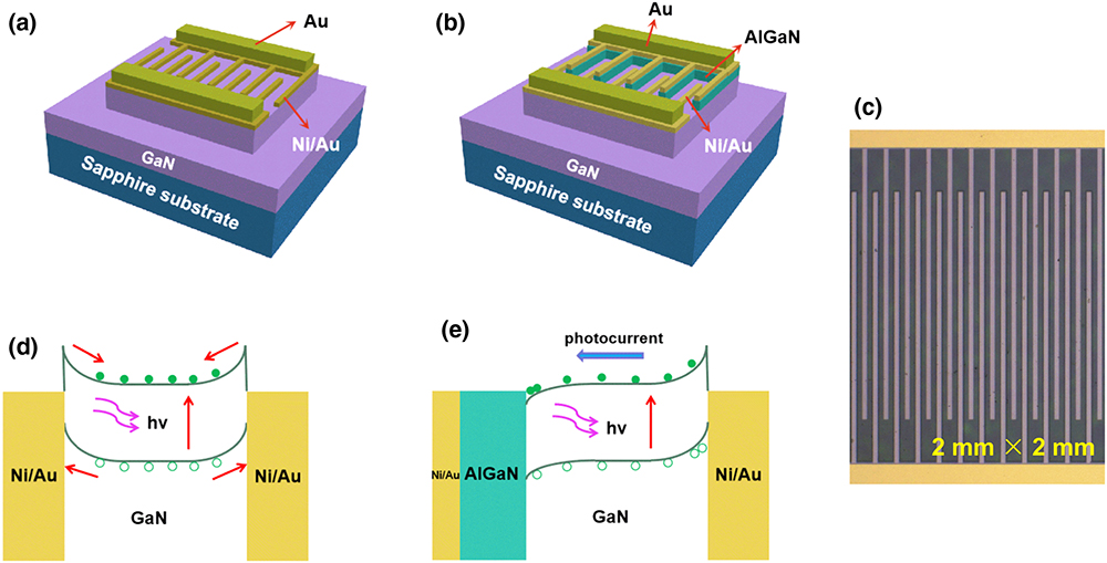
Figure 1.Schematic structures for (a) Device R and (b) Device N. (c) Top view of GaN-based MSM PD showing interdigital electrodes. Schematic energy band diagrams of (d) Device R and (e) Device N.
Figure 1(d) illustrates the schematic energy band diagrams of the traditional metal/GaN/metal PD structure for Device R. As is shown, the built-in electric fields generated by the two Schottky contacts are of the opposite directions, and the electrons can meet both energy barriers with the same energy barrier height; this energy band profile can strongly hinder the carrier diffusion, and we can also predict no current flow if Device R is not biased. However, when an
B. Sample Preparation
In the first step, the epilayers of Devices R and N are grown on AlN/sapphire templates by MOCVD. The trimethyl gallium (TMGa), trimethyl aluminum (TMAl), and ammonia (
C. Characterizations
![]()
Figure 2.(a) Dark current and photocurrent in terms of the applied bias for Devices R and N. Photocurrent for (b) Device R and (c) Device N in terms of different laser powers. (d) Two-dimensional electric field profiles and (e) current distributions for Devices R and N at the applied bias of 3 V under the 266 nm UV illumination. The bias is applied at the left electrode, such that the positive bias is biased at the left electrode in the first quadrant and the negative bias is biased at the left electrode in the second quadrant. The other electrode is grounded when the devices are measured. The wavelength for the illumination laser is 266 nm. The positive direction for the electric field is defined to point to the right side in (d).
D. Simulations
The APSYS calculations are carried out with a commercial software: Crosslight Software Inc. APSYS 2018 (http://www.crosslight.com), which can solve the continuity equation and Poisson equation by using the finite element method. The drift and diffusion processes for carriers can also be considered. The Shockley–Read–Hall (SRH) recombination lifetime is set to 10 ns [28]. The electron affinity for the Ni is set to 5.15 eV [29]. The polarization effect is considered at the
Absorption Coefficient of GaN Under Different Wavelengths
| Wavelength (nm) | Absorption Coefficient ( |
|---|---|
| 250 | |
| 260 | |
| 270 | |
| 280 | |
| 290 | |
| 300 | |
| 310 | |
| 320 | |
| 330 | |
| 340 | |
| 350 | |
| 360 | |
| 370 | |
| 380 | |
| 390 | |
| 400 |
3. RESULTS AND DISCUSSION
The dark current and the photocurrent as functions of the applied bias for the as-fabricated GaN-based MSM PDs are presented in Fig. 2(a). The bias is applied at the left electrode, such that the positive bias is biased at the left electrode in the first quadrant and the negative bias is biased at the left electrode in the second quadrant. The other electrode is grounded when the devices are measured. We have observed symmetric current-voltage characteristics for Device R, which agree with the energy band profile in Fig. 1(d). Nevertheless, the asymmetric current in terms of the applied bias is obtained for Device N, which is a signature for the unbalanced energy band profile as indicated in Fig. 1(e). The dark current for Device N is larger than that for Device R in the first quadrant, which means that the polarized
![]()
Figure 3.(a) Spectral responsivity, (b) and (c) energy band diagrams near the GaN layer surface, and (d) two-dimensional electric field profiles for Devices R and N at the applied bias of 0 V under 266 nm UV illumination.
In order to reveal the origin of the responsivity for Device N, we calculate and show the energy band diagrams for Devices R and N under 266 nm UV light illumination in Figs. 3(b) and 3(c), respectively. Note that both devices are not biased. In Fig. 3(b), we define two metal-semiconductor junctions as
![]()
Figure 4.Spectral responsivity for (a) Device R and (b) Device N at different applied biases.
A comparative chart is presented in Table 2, which summarizes the responsivity and peak wavelength for the reported GaN-based MSM PDs. It shows that the highest responsivity of
Performances for the Reported GaN-Based and AlGaN-Based PDs in the Literature
| Material | Responsivity | Wavelength (nm) | Self-powered | On/Off Ratio | Year | Refs. |
|---|---|---|---|---|---|---|
| GaN | 0.00154 A/W at 0 V | 340 | Yes | – | 2016 | [ |
| GaN | 3.096 A/W at 10 V | 360 | No | 2017 | [ | |
| 250 | No | 2017 | [ | |||
| GaN | 0.28 A/W at 10 V | 325 | Yes | 2018 | [ | |
| AlGaN | 0.115 A/W at 0 V, 0.154 A/W at 3 V | 270 | Yes | – | 2018 | [ |
| GaN | 0.633 A/W at 5 V | 325 | Yes | 2018 | [ | |
| 0.30 A/W at 8 V | 265 | No | 2019 | [ | ||
| GaN | 0.147 A/W at 3 V | 368 | No | 2019 | [ | |
| Ultra-thin GaN | 0.00176 A/W at 0 V | 325 | Yes | 2020 | [ | |
| 3.10 A/W at 30 V | 250 | No | 2020 | [ | ||
| GaN | 0.005 A/W at 0 V, 13.56 A/W at 3 V | 346 | Yes | 2021 | This work |
![]()
Figure 5.Time-dependent photo-response characteristics for (a) Device R and (b) Device N when devices are biased to 3 V. The laser wavelength is 266 nm.
4. CONCLUSIONS
In conclusion, we demonstrate the fabrication and the characterization of a self-powered GaN-based MSM UV PD. The self-powered GaN UV PD is realized by using the polarized
References
[1] L. Ravikiran, K. Radhakrishnan, N. Dharmarasu, M. Agrawal, Z. Wang, A. Bruno, C. Soci, T. Lihuang, K. S. Ang. GaN Schottky metal–semiconductor–metal UV photodetectors on Si(111) grown by ammonia-MBE. IEEE Sens. J., 17, 72-77(2017).
[2] N. Lu, Y. Gu, Y. Weng, Z. Da, Y. Ding. Localized surface plasmon enhanced photoresponse of AlGaN MSM solar-blind ultraviolet photodetectors. Mater. Res. Express, 6, 095033(2019).
[3] S. F. Chichibu, K. Shima, K. Kojima, S. Takashima, K. Ueno, M. Edo, H. Iguchi, T. Narita, K. Kataoka, S. Ishibashi, A. Uedono. Room temperature photoluminescence lifetime for the near-band-edge emission of epitaxial and ion-implanted GaN on GaN structures. Jpn. J. Appl. Phys., 58, SC0802(2019).
[4] M. Razeghi, A. Rogalski. Semiconductor ultraviolet detectors. J. Appl. Phys., 79, 7433-7473(1996).
[5] T. Yang, S. Chen, X. Li, X. Xu, F. Gao, L. Wang, J. Chen, W. Yang, X. Hou, X. Fang. High-performance SiC nanobelt photodetectors with long-term stability against 300°C up to 180 days. Adv. Funct. Mater., 29, 1806250(2019).
[6] Z. Xu, Y. Zhang, Z. Wang. ZnO-based photodetector: from photon detector to pyro-phototronic effect enhanced detector. J. Phys. D, 52, 223001(2019).
[7] J. Wang, L. Ye, X. Wang, H. Zhang, L. Li, C. Kong, W. Li. High transmittance β-Ga2O3 thin films deposited by magnetron sputtering and post-annealing for solar-blind ultraviolet photodetector. J. Alloy. Compd., 803, 9-15(2019).
[8] X. Li, C. Hemmingsson, U. Forsberg, E. Janzén, G. Pozina. Optical properties of AlGaN/GaN epitaxial layers grown on different face GaN substrates. Mater. Lett., 263, 127229(2020).
[9] Z. Alaie, S. M. Nejad, M. H. Yousefi. Recent advances in ultraviolet photodetectors. Mater. Sci. Semicond. Process., 29, 16-55(2015).
[10] M. Zhang, Y. Wang, F. Teng, L. Chen, J. Li, J. Zhou, X. Pan, E. Xie. A photoelectrochemical type self-powered ultraviolet photodetector based on GaN porous films. Mater. Lett., 162, 117-120(2016).
[11] A. Müller, G. Konstantinidis, M. Androulidaki, A. Dinescu, A. Stefanescu, A. Cismaru, D. Neculoiu, E. Pavelescu, A. Stavrinidis. Front and backside-illuminated GaN/Si based metal–semiconductor–metal ultraviolet photodetectors manufactured using micromachining and nano-lithographic technologies. Thin Solid Films, 520, 2158-2161(2012).
[12] W. Mou, L. Zhao, L. Chen, D. Yan, H. Ma, G. Yang, X. Gu. GaN-based Schottky barrier ultraviolet photodetectors with graded doping on patterned sapphire substrates. Solid-State Electron., 133, 78-82(2017).
[13] G. Wang, H. Lu, D. Chen, F. Ren, R. Zhang, Y. Zheng. High quantum efficiency GaN-based p-i-n ultraviolet photodetectors prepared on patterned sapphire substrates. IEEE Photon. Technol. Lett., 25, 652-654(2013).
[14] F. Wang. Theoretical study of back-illuminated separated absorption and multiplication AlGaN APDs with different structural parameters. Opt. Quantum Electron., 49, 216(2017).
[15] A. Gundimeda, S. Krishna, N. Aggarwal, A. Sharma, N. D. Sharma, K. K. Maurya, S. Husale, G. Gupta. Fabrication of non-polar GaN based highly responsive and fast UV photodetector. Appl. Phys. Lett., 110, 103507(2017).
[16] S. Chang, M. Chang, Y. Yang. Enhanced responsivity of GaN metal–semiconductor–metal (MSM) photodetectors on GaN substrate. IEEE Photon. J., 9, 6801707(2017).
[17] S. Rathkanthiwar, A. Kalra, S. V. Solanke, N. Mohta, R. Muralidharan, S. Raghavan, D. N. Nath. Gain mechanism and carrier transport in high responsivity AlGaN-based solar blind metal semiconductor metal photodetectors. J. Appl. Phys., 121, 164502(2017).
[18] T. H. Wood, J. Z. Pastalan, C. A. Burrus, B. C. Johnson, B. I. Miller, J. L. deMiguel, U. Koren, M. G. Young. Electric field screening by photogenerated holes in multiple quantum wells: a new mechanism for absorption saturation. Appl. Phys. Lett., 57, 1081-1083(1990).
[19] K. Shimomura. Proposal of field-effect-type photodetector using field-screening effect in the absorption of light. Jpn. J. Appl. Phys., 31, L1757-L1759(1992).
[20] F. Xie, H. Lu, X. Xiu, D. Chen, P. Han, R. Zhang, Y. Zheng. Low dark current and internal gain mechanism of GaN MSM photodetectors fabricated on bulk GaN substrate. Solid-State Electron., 57, 39-42(2011).
[21] S. K. Jain, S. Krishna, N. Aggarwal, R. Kumar, A. Gundimeda, S. C. Husale, V. Gupta, G. Gupta. Effect of metal contacts on a GaN/sapphire-based MSM ultraviolet photodetector. J. Electron. Mater., 47, 6086-6090(2018).
[22] D. Li, X. Sun, H. Song, Z. Li, H. Jiang, Y. Chen, G. Miao, B. Shen. Effect of asymmetric Schottky barrier on GaN-based metal-semiconductor-metal ultraviolet detector. Appl. Phys. Lett., 99, 261102(2011).
[23] X. Sun, D. Li, Z. Li, H. Song, H. Jiang, Y. Chen, G. Miao, Z. Zhang. High spectral response of self-driven GaN-based detectors by controlling the contact barrier height. Sci. Rep., 5, 16819(2015).
[24] M. Casalino, M. Iodice, L. Sirleto, I. Rendina, G. Coppola. Asymmetric MSM sub-bandgap all-silicon photodetector with low dark current. Opt. Express, 21, 28072-28082(2013).
[25] L. Dong, J. Yu, R. Jia, J. Hu, Y. Zhang, J. Sun. Self-powered MSM deep-ultraviolet β-Ga2O3 photodetector realized by an asymmetrical pair of Schottky contacts. Opt. Mater. Express, 9, 1191-1199(2019).
[26] L. Goswami, R. Pandey, G. Gupta. Ultra-thin GaN nanostructures based self-powered ultraviolet photodetector via non-homogeneous Au-GaN interfaces. Opt. Mater., 102, 109820(2020).
[27] T. Kabemura, S. Ueda, Y. Kawada, K. Horio. Enhancement of breakdown voltage in AlGaN/GaN HEMTs: field plate plus high-
[28] Z.-H. Zhang, S.-W. Huang Chen, Y. Zhang, L. Li, S.-W. Wang, K. Tian, C. Chu, M. Fang, H.-C. Kuo, W. Bi. Hole transport manipulation to improve the hole injection for deep ultraviolet light-emitting diodes. ACS Photon., 4, 1846-1850(2017).
[29] N. Miura, T. Nanjo, M. Suita, T. Oishi, Y. Abe, T. Ozeki, H. Ishikawa, T. Egawa, T. Jimbo. Thermal annealing effects on Ni/Au based Schottky contacts on n-GaN and AlGaN/GaN with insertion of high work function metal. Solid-State Electron., 48, 689-695(2004).
[30] M. Brendel, M. Helbling, A. Knigge, F. Brunner, M. Weyers. Measurement and simulation of top- and bottom-illuminated solar-blind AlGaN metal-semiconductor-metal photodetectors with high external quantum efficiencies. J. Appl. Phys., 118, 244504(2015).
[31] Z.-H. Zhang, L. Li, Y. Zhang, F. Xu, Q. Shi, B. Shen, W. Bi. On the electric-field reservoir for III-nitride based deep ultraviolet light-emitting diodes. Opt. Express, 25, 16550-16559(2017).
[32] J. F. Muth, J. D. Brown, M. A. L. Johnson, Z. Yu, R. M. Kolbas, J. W. Cook, J. F. Schetzina. Absorption coefficient and refractive index of GaN, AlN and AlGaN alloys. MRS Internet J. Nitride Semicond. Res., 4, 502-507(1999).
[33] D. Li, K. Jiang, X. Sun, C. Guo. AlGaN photonics: recent advances in materials and ultraviolet devices. Adv. Opt. Photon., 10, 43-110(2018).
[34] X. Sun, D. Li, H. Jiang, Z. Li, H. Song, Y. Chen, G. Miao. Improved performance of GaN metal-semiconductor-metal ultraviolet detectors by depositing SiO2 nanoparticles on a GaN surface. Appl. Phys. Lett., 98, 121117(2011).
[35] A. Yoshikawa, S. Ushida, K. Nagase, M. Iwaya, T. Takeuchi, S. Kamiyama, I. Akasaki. High-performance solar-blind Al0.6Ga0.4N/Al0.5Ga0.5N MSM type photodetector. Appl. Phys. Lett., 111, 191103(2017).
[36] N. Prakash, M. Singh, G. Kumar, A. Barvat, K. Anand, P. Pal, S. P. Singh, S. P. Khanna. Ultrasensitive self-powered large area planar GaN UV-photodetector using reduced graphene oxide electrodes. Appl. Phys. Lett., 109, 242102(2016).
[37] S. K. Jain, N. Aggarwal, S. Krishna, R. Kumar, S. Husale, V. Gupta, G. Gupta. GaN-UV photodetector integrated with asymmetric metal semiconductor metal structure for enhanced responsivity. J. Mater. Sci. Mater. Electron., 29, 8958-8963(2018).
[38] W. Y. Han, Z. W. Zhang, Z. M. Li, Y. R. Chen, H. Song, G. Q. Miao, F. Fan, H. F. Chen, Z. Liu, H. Jiang. High performance back-illuminated MIS structure AlGaN solar-blind ultraviolet photodiodes. J. Mater. Sci: Mater. Electron., 29, 9077-9082(2018).
[39] Y. P. Chen, C. H. Zheng, L. Q. Hu, Y. R. Chen. Improved performance of a back-illuminated GaN-based metal-semiconductor-metal ultraviolet photodetector by
[40] K. Jiang, X. Sun, Z.-H. Zhang, J. Ben, J. Che, Z. Shi, Y. Jia, Y. Chen, S. Zhang, W. Lv, D. Li. Polarization-enhanced AlGaN solar-blind ultraviolet detectors. Photon. Res., 8, 1243-1252(2020).
[41] Y. Wang, N. Yu. Fabrication visible-blind ultraviolet photodetector based on ZnS/GaN heterostructure with fast response. Mater. Express, 10, 629-633(2020).
[42] D. Guo, Z. Wu, P. Li, Y. An, H. Liu, X. Guo, H. Yan, G. Wang, C. Sun, L. Li, W. Tang. Fabrication of β-Ga2O3 thin films and solar-blind photodetectors by laser MBE technology. Opt. Mater. Express, 4, 1067-1076(2014).


Set citation alerts for the article
Please enter your email address

© Copyright 2018-2021 | Chinese Laser Press. All Rights Reserved 沪ICP备15018463号-20