Key Laboratory of Advanced Semiconductor Devices and Materials, School of Electronic Engineering, Xi’an University of Posts & Telecommunications, Xi’an 710121, China
Sn doping is an effective way to improve the response rate of Ga2O3 film based solar-blind detectors. In this paper, Sn-doped Ga2O3 films were prepared on a sapphire substrate by radio frequency magnetron sputtering. The films were characterized by X-ray diffraction, scanning electron microscopy, X-ray photoelectron spectroscopy and ultraviolet visible spectroscopy, and the effect of annealing atmosphere on the properties of films was studied. The Ga2O3 films changed from amorphous to β-Ga2O3 after annealing at 900 °C. The films were composed of micro crystalline particles with a diameter of about 5–20 nm. The β-Ga2O3 had high transmittance for wavelengths above 300 nm, and obvious absorption for solar-blind signals at 200–280 nm. The metal semiconductor metal type solar-blind detectors were prepared. The detector based on Sn-doped β-Ga2O3 thin film annealed in N2 has the best response performance to 254 nm light. The photo-current is 10 μA at 20 V, the dark-current is 5.76 pA, the photo dark current ratio is 1.7 × 10⁶, the response rate is 12.47 A/W, the external quantum efficiency is 6.09 × 10³%, the specific detection rate is 2.61 × 10¹² Jones, the response time and recovery time are 378 and 90 ms, respectively.
1. Introduction
The background radiation of the solar-blind ultraviolet signal (wavelength 200-280nm) is very low, and the interference from the sun can be almost ignored. It has the advantages of high detection sensitivity, strong anti-interference ability, and high communication accuracy, and is widely used in military, aerospace and civil fields[1-3]. Gallium oxide (Ga2O3) has a band gap of 4.4–5.3 eV, corresponding to 234–282 nm wavelength, which can cover the sun-blind band, making it a natural solar-blind detection material[4,5]. The cost of Ga2O3 single crystal substrates is very high. The preparation process of Ga2O3 nanomaterials is complex and difficult to produce in batches. Therefore, Ga2O3 thin film-based solar-blind detector has the most commercial application prospect[6]. The preparation methods of Ga2O3 thin films include metal-organic chemical vapor deposition (MOCVD)[7-9], molecular beam epitaxy (MBE)[10,11], atomic layer deposition (ALD)[12-14], pulse laser deposition (PLD)[15,16], plasma-enhanced chemical vapor deposition (PECVD)[17], radio frequency magnetron sputtering (RFMS)[18-21] and so on. The MOCVD, MBE, PLD and ALD methods can strictly control the thickness, composition, and doping concentration for high quality Ga2O3 thin films, but the equipment is complicated or the growth rate is relatively slow with a high production cost. PECVD has advantages such as low cost, high deposition rate, and good uniformity of film thickness, but it is difficult to achieve controllable doping. The RFMS method is challenging to obtain high quality single crystal Ga2O3 film, but the produced films have the advantages of good uniformity, high density, and strong adhesion. Besides, it has the advantages of simple equipment, easy operation, high deposition rate, low process cost and less environmental pollution, making it suitable for industrialization.
The Ga2O3 film prepared by the RFMS method is amorphous, and the obtained devices can exhibit obvious photoelectric response. For example, Zhanget al.[22] fabricated a deep ultraviolet photoelectric detector with a metal–semiconductor–metal (MSM) structure based on the amorphous Ga2O3 film prepared by RFMS. The fabricated device shows ultra-low dark current (1.41 × 10⁻¹¹ A), where the response rate is 1.77 A/W, and the response time is 114 ms. They believe that a large number of oxygen vacancies in the film can provide carriers and increase the responsiveness. Meanwhile, it is also the trap center of photo-generated carriers and increases the response time. Annealing treatment will reduce the oxygen vacancy concentration and improve the response speed, but at the same time, decrease the response rate. It has also been pointed out that the high resistivity of amorphous Ga2O3 films and the small photo-current of the solar-blind detector devices limit the response rate of the devices, such as the amorphous Ga2O3 films prepared by Li[23] using the RFMS method, with a photo-current of 0.846 nA and response rate of 0.12 mA/W at 30 V bias, and the photoelectric response of the annealedβ-Ga2O3 films disappeared. In contrast, the response rate of Sn-dopedβ-Ga2O3 films increased to 40 mA/W at 30 V. Both the undoped amorphous Ga2O3 andβ-Ga2O3 films prepared by the equipment used in this work have no obvious photoelectric response.
To increase the carrier concentration of Ga2O3 films, elements such as Sn can be used for doping. For example, Miet al.[24] prepared Sn-dopedβ-Ga2O3 thin films (Sn doping atomic ratio of 0−20%) on sapphire substrates using the MOCVD method, and the film resistivity decreased with increasing Sn doping concentration by five orders of magnitude when the doping concentration was 15%. Fenget al.[25] prepared Sn-dopedβ-Ga2O3 microfilaments by the conventional chemical vapor deposition technique, and prepared MSM photoelectric detectors based on a singleβ-Ga2O3 microwire, with a response rate of 12 A/W and external quantum efficiency of 5887%. Zhaoet al.[26] prepared Ga2–xSnxO3 (x = 0, 0.2, 0.6, 1.0) thin film solar-blind photo detectors using the L-MBE method, and under the same bias conditions, the response rate ofx = 0.2 sample to 254 nm light was several orders of magnitude higher than that ofx = 0 sample. Hou[27] prepared undoped and Sn-dopedβ-Ga2O3 film-based solar-blind UV detectors using MBE, and Sn doping increased the response rate of the devices from 8.11 to 127.89–444.51 A/W. We would use the RFMS method to prepare Sn-doped Ga2O3 thin films and investigate the effect of annealing atmosphere on the photoelectric detector performance. Using the RFMS method to develop photoelectric detectors with stable performance and high response is research with significance and application value.
In this paper, Sn-dopedβ-Ga2O3 thin film materials were prepared on a c-plane sapphire substrate using RFMS. The quality of the films was improved by annealing treatment. The structure and optical properties of Ga2O3 thin films were characterized using an X-ray diffractometer (XRD), field emission scanning electron microscope (SEM), energy dispersive spectrometer (EDS), X-ray photoelectron spectroscopy (XPS) and ultraviolet-visible (U-vis) spectroscopy. MSM type devices were prepared, the photoelectric response performance of the devices under 254 and 365 nm illumination was tested, and the corresponding working mechanism was analyzed.
2. Experiment
2.1. Materials and devices preparation
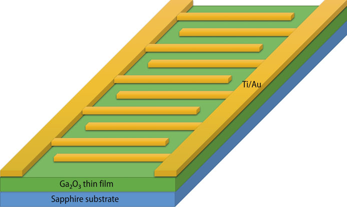
The 1.5 × 1.5 cm2 sapphire substrates were cleaned ultrasonically for 10 min using acetone, anhydrous ethanol, and deionized water in that order. The surface was blown dry with high purity N2. The films were deposited on the sapphire substrates using a Sn-doped Ga2O3 target (Ga2O3 : SnO2 = 95 : 5 at%), research RFMS method, setting the sputtering power to 140 W, sputtering gas of high-purity Ar2, gas flow rate to 40 sccm, working air pressure to 1.0 Pa, sputtering continuously at room temperature for 2 h. The produced films were annealed at 900 °C for 2 h in nitrogen (500 sccm) and air atmosphere respectively. Ti/Au (80 nm/50 nm thickness) interdigital electrodes (300µm in length, 50µm in width, and 30µm in pitch) were deposited on the prepared Ga2O3 films using standard lithography and electron beam evaporation process. The MSM type solar-blind photoelectric detectors had been prepared based on Ga2O3 films, and the device structure is shown inFig. 1.
Figure 1.(Color online) Schematic diagram of solar-blind photodetector with MSM structure.
The structural properties were characterized by the X-ray diffraction (XRD, model: Bruker D8 Advance). The surface morphology and thickness of the films were tested by a scanning electron microscope (SEM, model: JSM-7610FPlus). The chemical composition of the films was determined by the X-ray photoelectron spectroscopy (XPS, model: Thermo SCIENTIFIC ESCALAB Xi+). The transmission spectra of the Ga2O3 films were measured by ultraviolet-visible spectroscopy (UV-vis, model: UV-2400), and theI–V andI–t electrical properties of the solar-blind photoelectric detectors under different photo conditions were tested by a semiconductor device analyzer (model: Keysight 1505).
3. Result and discussion
Fig. 2 shows the XRD patterns of the unannealed, annealed in nitrogen and annealed in air Ga2O3 films, the test method was grazing incidence, and the incidence angle was 1°. The unannealed film had no obvious diffraction peaks and only had large wave packets in the diffraction angle range of 20°–40°, which indicate that the crystalline quality of the films grown under this condition was poor. After annealing in nitrogen or air, sharp diffraction peaks were observed, indicating that the crystal quality was significantly improved. There were three strongest diffraction peaks located at 30.41°, 31.52° and 64.81°, corresponding to the [−401], [−202] and [−712] crystal orientation ofβ-Ga2O3 (JCPDS Card No. 87-1901), while the other obvious diffraction peaks belong toβ-Ga2O3 too. The diffraction peaks of the sapphire substrate and tin were not found in the figures, indicating that the films were uniform and dense, and the tin dopants were well dissolved in Ga2O3 without the second-phase segregation, or the concentration of second-phase was lower than the testing accuracy of XRD.
Figure 2.(Color online) XRD spectrum of Ga2O3 films.
Figs. 3(a)–3(c) show the SEM surface and cross-sectional images of Ga2O3 films: unannealed, annealed in nitrogen atmosphere, and annealed in air atmosphere. It can be seen that the surface of the unannealed film was composed of tiny particles about 5–20 nm in diameter, with a uniform thickness of about 278 nm and a good bond with the substrate. After annealing in nitrogen atmosphere, the size of the tiny particles was more uniform, and the thickness of the film slightly increased to about 300 nm. Due to the lattice mismatch between the Ga2O3 film and the substrate, and the different thermal expansion coefficients at high temperatures, the adhesion between the film and the substrate was reduced. The uneven thickness of the film after being annealed in an air atmosphere was probably due to the reaction between oxygen in the air and the film at high temperatures.
Figure 3.(Color online) SEM of Ga2O3 thin films: (a) unannealed, (b) annealed in nitrogen, (c) annealed in air. (d) EDS spectra of Ga2O3 thin films.
From the results of XRD, it can be seen that high-temperature annealing makes the film transform from amorphous to polycrystalline. In the process of crystallization, the annealing atmosphere had a certain effect on regulating the atomic percentages of gallium, oxygen and tin. As shown in the EDS results (Fig. 3(d)), the peaks of Sn elements existed in all three Ga2O3 film samples. Sn ions may be a substitution or interstitial doped in Ga2O3. The atomic ratios of Ga : Sn were 40.8 : 1 (unannealed), 48.9 : 1 (N2 annealed) and 43.1 : 1 (air annealed) respectively, Sn decreased after annealed both in N2 and air, and Sn content was lower in the N2 annealed sample. The atomic ratios of O : Ga were much greater than 3 : 2, so there were many other absorbed oxides on the surface of Ga2O3 films, including physical adsorption and chemical adsorption, such as carbon, hydrogen or others.
To reveal the chemical bonding states and compositions in thin films, the typical XPS survey spectra of the unannealed, annealed in N2 and annealed in air Ga2O3 thin films were shown inFig. 4(a), which were dominated by the spectra of Ga (2s, 2p, 3s, 3p, 3d), Sn 3d, O 1s and C 1s, the auger peaks from the gallium (Ga LM1,Ga LM2) and the oxygen (O KL1) were clearly observed too[28-30]. The peak of Ga 3d at 20.4 eV indicates the lattice Ga–O bond in the Ga3+ oxidation state, and the weak O 2s peak was observed at the 23.1 eV, as shown inFig. 4(b)[28,31].Fig. 4(c) shows the typical Sn 3d peaks at ~495.1 eV (3d3/2) and ~486.7 eV (3d5/2) with an energy difference of ~8.4 eV from the Sn4+ oxidation state corresponding to its substitution on the lattice Ga site[28,30]. The peak at ~ 491.4 eV was also detected due to the 3d core level of metal Sn (Sn0). The existence of Sn0 indicated that Sn dopants were not fully oxidized[28]. The peak area ratios of Sn4+:Sn0 were 42.5% : 57.5% (unannealed), 55.6% : 44.4% (N2 annealed) and 57.4% : 42.6% (air annealed). O 1s XPS spectra of Sn-doped Ga2O3 films were resolved into three components centered at 530.6, 531.4, and 532.1 eV for lattice oxygen (Ga–O and Sn–O bonds), oxygen vacancy, and O–H (C–O) bonds, respectively[28-32] (as shown inFig. 4(d)). The peak area ratios of lattice oxygen : oxygen vacancy : O–H (C–O) were 38.5% : 48.8% : 12.7% (unannealed), 64.1% : 12.2% : 23.7% (N2 annealed) and 71.4% : 11.4% : 17.1% (air annealed) respectively. The concentration of lattice oxygen increased and oxygen vacancy decreased during the crystallization of the film. The ratio of O–H (C–O) increased in the N2 annealed sample and decreased in the air annealed sample, which caused the changes of oxygen concentration, in agreement with the EDS results.
Figure 4.(Color online) The XPS analysis for the Ga2O3 thin films: (a) survey peaks, (b) Ga 3d spectra, (c) Sn 3d spectra, and (d) O 1s spectra.
It can be speculated that high-temperature annealing made the process of crystallization of the films, the oxygen vacancies and atomic ratio of Sn reduced after annealing both in N2 and air atmosphere, while the Sn4+ substitution doping ratio increased.
Fig. 5(a) shows the transmission spectra of Ga2O3 films: unannealed, N2 annealed and air annealed, with wavelengths set from 200 to 800 nm. At 365 nm, the transmittance of the unannealed sample dropped to 73%. In the 250–300 nm range, the transmittance of all three samples dropped sharply, indicating that the samples absorbed light in this wavelength range significantly. A plot of (αhν)2–hν is shown inFig. 5(b), where the absorption coefficientα is derived using Eq. (1)[33]:
Figure 5.(Color online) (a) Transmission spectra of Ga2O3 thin films. (b) The plot of (αhν)2–hν.
whereτ is the thickness value of the film andT is the transmittance. After the absorption coefficient is derived, it is brought into Eq. (3):
whereh is Planck's constant,ν is the incident photon frequency andλ is the wavelength.n is taken as 1/2 andEg is the band gap of the semiconductor material. The band gaps of the unannealed, N2 annealed, and air annealed samples were estimated to be 4.86, 4.94 and 4.89 eV, respectively. The band gap increased due to the reduction of Sn atomic ratio after annealing. The N2 annealed sample had the best crystalline quality and the largest band gap.
Figs. 6(a)–6(c) show theI–V characteristic curves of the photoelectric detectors made from three thin film samples, unannealed, annealed in nitrogen and air atmosphere, respectively. The detectors after annealed exhibited good Ohmic contact in the bias voltage range of –20 to 20 V, and the current shows a good linear relationship with the bias voltage.Fig. 6(a) shows theI–V curves under dark conditions, the three samples had dark current of pA level at 20 V, and the current-voltage curve slightly deviates from Ohm's law.Figs. 6(b) and6(c) show theI–V curves of the fabricated devices under 254 and 365 nm illumination, with currents ofμA level and nA level respectively.Figs. 7(a)–7(c) show the logarithmic curves of the photo current and dark current of the devices at –20 to 20 V bias voltage, from which it can be seen that the photo-to-dark current ratio (PDCR) of the unannealed and annealed in air atmosphere devices at 20 V bias voltage were 105, while the PDCR of the annealed in nitrogen device was 106.
Figure 6.(Color online) (a) I–V curve in dark condition. (b) I–V curve at 254 nm wavelength illumination. (c) I–V curve at 365 nm wavelength illumination of Ga2O3 thin films.
Figure 7.(Color online) Photocurrent at 254, 365 nm illumination and dark current logarithmic curves of Ga2O3 thin films: (a) unannealed, (b) annealed in nitrogen, (c) annealed in air.
In comparison, the unannealed device had the minimum dark current and photo current at 254 nm illumination, and the maximum photo current at 365 nm illumination. The dark current of the annealed devices increased because the crystalline quality of the films improved, making the carrier mobility higher. The dark current of the nitrogen annealed device was smaller than that of the air annealed device due to the lower Sn doping concentration. There were strong grain boundary potential barriers in polycrystalline Ga2O3 films, resulting in the dark current as low as the pA level. At 254 nm illumination, a large number of photogenerated carriers reduced the grain boundary potential barrier, causing the photocurrent up toμA level. The photo current of the nitrogen annealed device was maximum. This may be due to the fact that the quality of films annealed in nitrogen atmosphere was better, the grain size and thickness distribution were uniform, and the excited carriers were less scattered by lattice and grain boundary, meanwhile, slightly higher concentration of oxygen vacancy might provide more carriers. The unannealed device had the smallest band gap and the lowest transmittance to 365 nm illumination, thus absorbing more energy, causing obvious photocurrent, while the nitrogen annealed device had the minimum photo current at 365 nm illumination, due to the lowest Sn doping concentration and largest band gap. It can be inferred that Sn doping reduced the selectivity properties of the detector to the solar-blind signals.
All three solar-blind photoelectric detectors had certain responses to 365 nm light, and more significantly, to 254 nm light. The photo-current of the nitrogen annealed device was 10μA at 254 nm illumination and 20 V bias voltage conditions (dark current was 5.76 pA at 20 V), PDCR was 1.7 × 10⁶, while the response to the 365 nm photo was the weakest. It can be inferred that the nitrogen annealed device had the best response rate and selectivity to solar-blind signals.
However, the photo-current of the undoped Ga2O3 films prepared by the same process was nearly the same as their dark-current. The photoelectric responses of Sn-doped Ga2O3 films were significantly improved, indicating that Sn doping effectively increased the carrier concentration and reduced the grain boundary potential barrier.
Figs. 8(a)–8(c) show theI–t curves of the three Ga2O3 solar-blind photoelectric devices under 20 V bias voltage for unannealed, annealed in nitrogen and air atmosphere, respectively. By setting the switching duration of the 254 nm photo source to 5 s, the devices showed good consistency over multiple photo-dark cycles, indicating that the devices had good stability and repeatability.Figs. 8(d)–8(f) are partial images ofFigs. 8(a)–8(c), respectively, which show the response (τr) and recovery (τd) time characteristics of the devices to light. The response and recovery time of the unannealed device could be divided into two periods, the fast response period and the slow response period, so the time was longer,τr was 540 ms, andτd was 600 ms.τr for the air atmosphere annealed device was 390 ms andτd was 124 ms;τr for the nitrogen atmosphere annealed device was 378 ms andτd was 90 ms. It can be inferred that nitrogen atmosphere annealing was an effective way to improve the response and recovery speed of the device.
Figure 8.(Color online) I–t curves of Ga2O3 solar-blind photoelectric devices: (a) unannealed, (b) annealed in nitrogen, (c) annealed in air, (d) unannealed (part of (a)), (e) annealed in nitrogen (part of (b)), (f) annealed in air ((part of (c)).
Fig. 9 shows the PDCR curve of the devices unannealed, nitrogen annealed and air annealed with a bias voltage range of –20 to 20 V. The PDCR of the devices was above 105 in most voltage ranges. The PDCR varied slightly in the ranges of –20 to –7 V and 4 to 20 V, indicating that the photodetectors had a wide operating voltage range and could maintain high sensitivity at smaller driving voltages. When measuring the dark current, the contact resistances between the two electrodes and the material below the electrodes were large and slightly different, which caused the current–voltage curve to deviate from Ohm's law (as shown inFig. 6(a)). When measuring the photo current, the symmetry of the curve was good, due to the reduction of the contact resistances. Therefore, the PDCR of the unannealed, nitrogen atmosphere annealed and air atmosphere annealed devices achieve the maximum at –3.6, –2.4, and –2 V respectively.
Figure 9.(Color online) Curve of photo-dark current ratio (PDCR) changing with bias voltage.
In addition, the response rate (R), external quantum efficiency (EQE) and detection rate (D*) are also three important pieces of data in the performance of solar-blind detection devices. The response rate is obtained from Eq. (4)[34]:
whereP254 is the optical power density of 254 nm UV (10 W/m2) andS is the effective area (8.1 × 10⁻⁸ m2). The external quantum efficiency is given by Eq. (5)[34]:
wherec is the speed of light, andq is the total electronic charge. As a parameter characterizing the ability of the device to detect noisy optical signals, the specific detection rate is given by Eq. (6)[35]:
Under 254 nm UV illumination and 20 V bias voltage, the calculated results are shown inTable 1. Among them, the nitrogen annealedβ-Ga2O3 thin film solar-blind photoelectric detector had the best performance: PDCR (1.75 × 10⁶),R (12.47A/W), EQE (6.09 × 10³%),D* (2.61 × 10¹²Jones),τr/τd(0.39 s/0.12 s). It is worth noting that the distance between interdigital electrodes of the photoelectric devices prepared in this paper is 30µm, and the distance can be further reduced to obtain a higher response and detection rate. At present, there have been a large number of relevant research reports[36-48] and reviews[49,50] on gallium oxide solar-blind photoelectric detection devices. The performance indicators of some devices are listed inTable 1. Compared with the literature, the devices made in this work had a good comprehensive performance.
4. Conclusion
In this paper, Sn-doped Ga2O3 films were prepared by the RFMS method, and photoelectric detectors were fabricated by photolithography, electron beam evaporation and other processes. The experiment results show that the three kinds of photoelectric detectors have good repeatability and stability, and have obvious response to 254 nm light. The PDCR value is 105 or higher, and the response to 365 nm light is weak, and the response and recovery time are less than 1 s. Sn doping effectively increased the carrier concentration and reduced the grain boundary potential barrier, but also reduced the selectivity of the detectors to the solar-blind signals.
However, among the three as produced devices, the nitrogen annealed device has the lowest Sn concentration, the largest band gap, and the best comprehensive performance. The high-temperature nitrogen atmosphere annealing may be an effective method to reduce defects and improve the crystalline quality of the film. In addition, this work did not compare the samples with different doping concentrations and did not explore the best Sn doping concentration for solar-blind photoelectric detection performance.
In summary, the device fabricated by the nitrogen annealed film has excellent performance (the photo-current is 10μA and the dark-current is 5.76 pA at 20 V, PDCR is 1.7 × 10⁶, response rate is 12.47 A/W, response time is 378 ms, and recovery time is 90 ms). This prepared by the RFMS method. The Sn-doped Ga2O3 thin film based solar-blind photoelectric detector has a low cost, high response rate and stable performance, and has promising practical application prospects.
The Author Email: Li Lijun (lilijun007@163.com), Li Chengkun (lilijun007@163.com), Wang Shaoqing (lilijun007@163.com), Lu Qin (lilijun007@163.com), Jia Yifan (lilijun007@163.com), Chen Haifeng (lilijun007@163.com)