• Acta Photonica Sinica
  • Vol. 52, Issue 8, 0823001 (2023)
Xiaowei YANG, Weifang YUAN, Tonghui LI, Yu LI, Xiaowen DONG, Kai LIU, Yongqing HUANG, and Xiaofeng DUAN*
Author Affiliations
  • State Key Laboratory of Information Photonics and Optical Communications,Beijing University of Posts and Telecommunications,Beijing 100876,China
  • show less
    DOI: 10.3788/gzxb20235208.0823001 Cite this Article
    Xiaowei YANG, Weifang YUAN, Tonghui LI, Yu LI, Xiaowen DONG, Kai LIU, Yongqing HUANG, Xiaofeng DUAN. Design and Fabrication of Integrated Microlens for High Speed Photodetectors[J]. Acta Photonica Sinica, 2023, 52(8): 0823001 Copy Citation Text show less

    Abstract

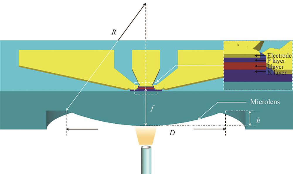
    With the accelerated development of new industries such as big data and cloud computing, higher requirements are put forward for the capacity of communication networks. Due to the limitations of electrical interconnection, optical interconnection occupies an increasing proportion in the communication system. In order to meet the demand of rapid increase of optical communication network capacity, improving the transmission rate of single channel is an effective solution. Therefore, high speed optical detector is widely used in optical communication system. The goal of high speed optical detector is to obtain a higher bandwidth of 3 dB, and reducing the surface area of the device is an effective way to achieve it. The decrease of the mesa area can reduce the junction capacitance of the optical detector and thus improve the bandwidth of the optical detector. However, the decrease of the mesa area can reduce the optical coupling efficiency of the optical detector and directly increase the optical coupling loss in the system. To solve this problem, the monolithic integrated microlens structure on the back of high speed optical detector substrate is an effective solution. The structure increases the equivalent photosensitive surface of the optical detector, increases the optical coupling efficiency of the optical detector, and can effectively compensate the alignment deviation. An InP-based microlens structure integrated with a 1.31 μm optical detector chip is designed for data center applications. An InP-based microlens structure integrated with a 1.31 μm optical detector chip is designed for data center applications. An experimental method was developed to fabricate microlens glue by hot melt and transfer microlens glue by Inductively Coupled Plasma (ICP) etching. SiCl4 and Ar were selected as etching gases in ICP etching process to ensure the safety of the experiment. An InP-based microlens with diameter of 90.3 μm, crown height of 18.5 μm and smooth surface morphology was prepared. In this paper, a single InP microlens integrated on the back of the optical detector is designed, simulated and fabricated, which can improve the optical coupling efficiency of the device and compensate the alignment deviation. Through software simulation, the microlens with a diameter of 100 μm and a crown height of 18 μm can realize the convergence function at the focal length of 114 μm under two light incident angles of collimation and divergence of 10°, which meets the requirement of integration on the back of the optical detector. To prepare the microlens, the adhesive shape is first made, and then the adhesive shape is transferred to the substrate by etching to form the microlens. The adhesive shape of the microlens is made by photoresist hot melt method. Photoresist hot melt method is a common technology for microlens preparation. It can be used to produce microlens adhesive with the morphology and size meeting the requirements by using standard semiconductor equipment and technology. The method has high repeatability, good homogeneity and low cost. The microlens adhesive with smooth surface and no depression was prepared by photoresist hot melt method. The relatively safe SiCl4 and Ar were used for etching gas. By studying the influence of cavity pressure, etching gas flow and RF power on ICP etching, the ICP etching conditions of SiCl4 flow 13 sccm, Ar flow 13 sccm, pressure 0.266 Pa in the reaction cavity and RF power 105 W were finally selected. The InP microlens with diameter of 90.3 μm, arch height of 18.5 μm and smooth surface morphology was prepared. The responsivity of PIN light detector with backside monolithic integrated microlens was tested by source meter, optical fiber and probe station under incident light with wavelength of 1.31 μm. In the test process, the optical signal output by the laser with wavelength of 1.31 μm is incident into the optical detector through the fiber. The electrical signal generated by the optical detector enters the source table through the high-frequency line, changes the optical output power of the laser and records the corresponding optical current value on the source table, and finally calculates the responsiveness of the PIN optical detector. When the incident light of 1.31 μm wavelength is incident in the direction of 3° from the main optical axis, the response of the PIN light detector decreases by 4%. The prepared InP microlens meets the design requirements.
    Xiaowei YANG, Weifang YUAN, Tonghui LI, Yu LI, Xiaowen DONG, Kai LIU, Yongqing HUANG, Xiaofeng DUAN. Design and Fabrication of Integrated Microlens for High Speed Photodetectors[J]. Acta Photonica Sinica, 2023, 52(8): 0823001
    Download Citation