• Journal of Semiconductors
  • Vol. 40, Issue 5, 052201 (2019)
Yan Gao1、2, Liyun Zhao2、3, Qiuyu Shang2、3, Chun Li2, Zhen Liu2, Qi Li1, Xina Wang1, and Qing Zhang2、3
Author Affiliations
  • 1Hubei Collaborative Innovation Center for Advanced Organic Chemical Materials, Hubei Key Laboratory of Ferro & Piezoelectric Materials and Devices, Faculty of Physics and Electronic Science, Hubei University, Wuhan 430062, China
  • 2Department of Materials Science and Engineering, College of Engineering, Peking University, Beijing 100871, China
  • 3Research Center for Wide Gap Semiconductor, Peking University, Beijing 100871, China
  • show less
    DOI: 10.1088/1674-4926/40/5/052201 Cite this Article
    Yan Gao, Liyun Zhao, Qiuyu Shang, Chun Li, Zhen Liu, Qi Li, Xina Wang, Qing Zhang. Photoluminescence properties of ultrathin CsPbCl3 nanowires on mica substrate[J]. Journal of Semiconductors, 2019, 40(5): 052201 Copy Citation Text show less

    Abstract

    Fabricating high-quality cesium lead chloride (CsPbCl3) perovskite nanowires (NWs) with dimension below 10 nm is not only of interests in fundamental physics, but also holds the great promise for optoelectronic applications. Herein, ultrathin CsPbCl3 NWs with height of ~7 nm, have been achieved via vapor phase deposition method. Power and temperature-dependent photoluminescence (PL) spectroscopy is performed to explore the emission properties of the CsPbCl3 NWs. Strong free exciton recombination is observed at ~3.02 eV as the temperature (T) is 78-294 K with binding energy of ~ 37.5 meV. With the decreasing of T, the PL peaks exhibit a first blueshift by 2 meV for T ~ 294-190 K and then a redshift by 4 meV for T ~ 190-78 K. The exciton–optical phonon interaction plays a major role in the linewidth broadening of the PL spectra with average optical phonon energy of ~48.0 meV and the interaction coefficient of 203.9 meV. These findings advance the fabrication of low dimensional CsPbCl3 perovskite and provide insights into the photophysics of the CsPbCl3 perovskite.

    1. Introduction

    Lead halide perovskites hold great promises in the field of optoelectronic devices, due to their excellent optical and electrical properties including high optical gain, stable excitonic luminescence, fast carrier mobility and high fluorescence quantum efficiency[16]. Among the family of perovskites, all-inorganic lead hailed perovskites (CsPbX3, X = Cl, Br, I) have attracted much attention due to their relatively better thermal stability[7, 8]. Up till now, tremendous efforts have been devoted to cesium lead bromine (CsPbBr3) perovskite and great successes have been obtained in the fields of light-emitting diodes (LEDs), lasers, photodetectors and solar cells, etc.[913]. The chloride counterpart, cesium lead chloride (CsPbCl3), a wide bandgap semiconductor, has also demonstrated outstanding optoelectronic responses[1416]. For example, CsPbCl3 nanocrystal photodetector exhibits a high detective sensitivity up to 2 × 10¹³ Jones, ultraviolet response exceeding 106 A/W and a good ambient stability lasting for 2400 h with degradation less than 10%[17]. One dimensional nanowire (NW) of CsPbCl3 is promising for the blue color micro-LED and laser, etc. For example, the strong lasing action at 424 nm has been observed in single-crystal CsPbCl3 NWs at room temperature[8, 18]. However, most of these works focus on the NWs with height of several hundred nanometers. The emission properties and fabrication of CsPbCl3 NWs in quantum confinement regime are still inadequate.

    In this work, ultrathin CsPbCl3 NW arrays on mica substrate are achieved by chemical vapor deposition (CVD) method. Power- and temperature-dependent photoluminescence (PL) spectroscopy is carried out to investigate emission dynamics of the as-prepared CsPbCl3 NWs. Strong PL peak is observed at ~ 3.02 eV with full width at half maximum (FWHM) of ~ 58 meV owing to the free exciton (FX) recombination. With temperature decreasing from 294 to 77 K, the PL peak shows a first blueshift and then redshift at a transition temperature of ~ 190 K. The temperature dependence of intensity and FWHM of FX peak is fitted by Arrhenius equation and Boson models with an exciton binding energy and average optical phonon energy of ~ 37.5 and ~ 48.0 meV, respectively. These results advance the understanding of exciton properties of CsPbCl3.

    2. Experiment details

    In this work, the atomically-flat muscovite mica KAl2(AlSi3O10)(OH)2 was used as growth substrate[8]. The mixed CsCl and PbCl2 powders (99.99%, purchased from Sigma Aldrich) of ~ 1 : 1 molar ratio were used as precursors. The growth temperature and duration time are set as ~ 620 °C and 15 min, respectively. The whole growth proceeding was accompanied by high purity carrier gas N2 with flow rate of ~ 30 sccm. The morphologies and structures are characterized by scanning electron microscopy (SEM), atomic force microscopy (AFM) and X-ray diffraction (XRD). For steady-state PL spectroscopy measurement of CsPbCl3 NWs, the 360 nm continuous-wave laser was used as excitation source and focused onto NWs by a 10 × objective (NA = 0.25). The PL signal was collected by a reflective symmetry with the same objective and analyzed by a monochromator equipped with a liquid nitrogen cooled charge coupled detector. For low temperature PL spectroscopy, the mica deposited with NWs was put into a continuous-flow micro-cryostat with liquid nitrogen.

    3. Results and discussions

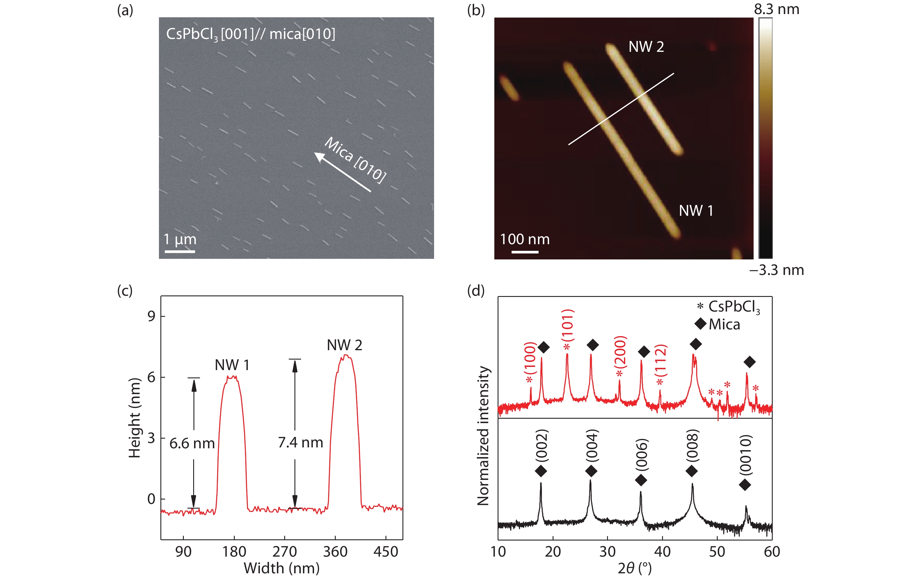
    The SEM image (Fig. 1(a)) shows that the as-grown NWs are well arranged along the [010] direction of the mica substrate. The NW length varies from tens to several hundreds of nanometers. The AFM image (Fig. 1(b)) shows that the NWs exhibit homogenous morphology along the long axis of NWs, suggesting the good crystallinity of the as-grown NWs. The heights of the two representative NWs (Fig. 1(c)) are ~ 6.6 and 7.4 nm, respectively, much smaller than that reported in the previous works[19]. XRD with Cu radiation source (Kα1, λ = 1.5406 Å) was conducted to study the crystal phase of the CsPbCl3 NWs at 294 K (Fig. 1(d)). Four strong diffraction peaks are observed at 16.0°, 22.6°, 32.1° and 39.5°, corresponding to the (100), (101), (200) and (112) faces, respectively, suggesting the tetragonal-phase of CsPbCl3 perovskite (JCPDS no. 18-0366)[20]. In addition, the diffraction peaks at 17.8°, 26.8°, 36.0°, 45.4°, 55.2° can be attributed to (002), (004), (006), (008) and (0010) faces of mica[21]. Since there is a large lattice mismatch between the (100)-face CsPbCl3 and mica (001) (dmica (100) = 5.189 Å, dmica (010) = 8.995 Å, JCPDS no. 06-0623; dCsPbCl3(100) = dCsPbCl3(010) = 5.584 Å, dCsPbCl3(001) = 5.623 Å, JCPDS no. 18-0366), the growth dynamics of CsPbCl3 NWs on mica is driven by an incommensurate epitaxy mechanism[19]. Two potential incommensurate epitaxy models are considered: (1) CsPbCl3 [010] ‖ mica [010] and CsPbCl3 [001] ‖ mica [100], and the corresponding lattice mismatch factorf, expressed as f = (1 − dsample/dsubstrate) × 100%, is ~ 0.67% (8dCsPbCl3(010) ≈ 5dmica(010)) and ~ 2.47 % (9dCsPbCl3(001) ≈ 10dmica(100)); (2) CsPbCl3 [001] ‖ mica [010] and CsPbCl3 [010] ‖ mica [100], and the correspondingfare ~ −0.02% (8dCsPbCl3(001) ≈ 5dmica(010)) and ~ 3.15% (9dCsPbCl3(010) ≈ 10dmica(100))[11, 19]. The second model has lower lattice match and hence is energetically preferred.

    (Color online) The structure and morphology characterization of ultrathin CsPbCl3 nanowires (NWs) epitaxial on mica. (a) Scanning electron microscopy (SEM) image of the ultrathin CsPbCl3 NWs grown on (001)-mica by chemical vapor deposition method. (b) Atomic force microscopy (AFM) image of the CsPbCl3 NWs, scale bar: 100 nm. (c) Corresponding data of CsPbCl3 NWs height extracted from (b). (d) X-ray diffraction pattern of the CsPbCl3 NWs on mica (red line) and mica (black line).

    Figure 1.(Color online) The structure and morphology characterization of ultrathin CsPbCl3 nanowires (NWs) epitaxial on mica. (a) Scanning electron microscopy (SEM) image of the ultrathin CsPbCl3 NWs grown on (001)-mica by chemical vapor deposition method. (b) Atomic force microscopy (AFM) image of the CsPbCl3 NWs, scale bar: 100 nm. (c) Corresponding data of CsPbCl3 NWs height extracted from (b). (d) X-ray diffraction pattern of the CsPbCl3 NWs on mica (red line) and mica (black line).

    Fig. 2 shows PL spectra of CsPbCl3 NWs under the excitation of 360 nm continuous-wave laser at 294 and 78 K, respectively. At 294 K, two peaks can be resolved for both the as-grown CsPbCl3 thin NW (height: ~ 7 nm with a ~ ±2.0 nm; Fig. 2(a), upper panel) and the bulk-like wire (thick NW, height: ~ 8 μm; Fig. 2(a), lower panel). The high and low-energy peak can be well fitted by Lorentzian functions (solid black curves). For the thin NW, the high-energy peak locates at ~ 3.023 eV (FWHM, ~ 58 meV) and dominates the whole PL spectroscopy, which is primarily attributed to FX emission considering the high exciton binding energy of the CsPbCl3[22-24]. A low-energy peak at ~ 2.953 eV, indicated as X-band, is observed with lower intensity and larger FWHM (~174 meV). It should be noted that the as-measured FX emission energy of the thin NWs can vary in the range of ~ 3.020–3.028 eV at 294 K owing to the fluctuation the NW dimension across the mica substrate. The FX and X-band emission of the bulk-like CsPbCl3 wire locate at ~ 2.993 and 2.945 eV, respectively; both of them are smaller than that of the thin NWs, suggesting the existence of quantum confinement effect in the thin NWs. Similar phenomena are observed at 78 K (Fig. 2(b)). The FX and X-band emission band locate at ~ 3.021 and ~ 2.967 eV for the thin NW, respectively, which are higher than that of the bulk-like wire (FX: ~ 3.001 eV; X-band: ~ 2.973 eV). Moreover, the X-band emission is easier to be resolved at 78 K compared to 294 K, indicating that the binding energy of the associated excitons is smaller than that of the FX.

    (Color online) Photoluminescence (PL) emission spectra of thin (height: ~ 7 nm; upper panel) and thick (height: ~ 8 μm; lower panel) CsPbCl3 NWs on mica at (a) 294 K and (b) 78 K, respectively. Solid and dashed lines: Lorentzian function fitting curves; open circles: experimental data. The excitation power density Pex of ~ 1.2 kW/cm2.

    Figure 2.(Color online) Photoluminescence (PL) emission spectra of thin (height: ~ 7 nm; upper panel) and thick (height: ~ 8 μm; lower panel) CsPbCl3 NWs on mica at (a) 294 K and (b) 78 K, respectively. Solid and dashed lines: Lorentzian function fitting curves; open circles: experimental data. The excitation power density Pex of ~ 1.2 kW/cm2.

    Power-dependent PL spectroscopy is performed to further study the origin of PL peaks in the thin NW at 294 K (Fig. 3(a)). As the excitation power density Pex increases from ~ 0.3 to 61.1 kW/cm2, the FX emission primarily dominates the PL spectroscopy, suggesting that FX recombination is the major radiative transition channel for the thin NW. The integrated PL intensity IP versus Pex is extracted which can be well fitted by the equation of IPPexα (Fig. 3(b))[25]. As the power law α< 1, the radiative transition process involves an impurity, such as donor-acceptor pair recombination; for 1 <α< 2, it usually belongs to excitonic transition process (free- or bound-exciton emission); forα≈ 2, it is for electron-hole bimolecular recombination[25, 26]. For the FX emission, the power law α is ~ 1.05, which is good consistent with the recombination of FX. The power law αis 1.38 for the X-band emission, which is larger than the FX and also suggesting an excitonic emission. Considering that the binding energy of the exciton associated with the X-band is lower than the FX, we attributed the X-band emission to the recombination of trions or other types of bound excitons, which would be studied in the further works[25, 27]. Nevertheless, α is nearly ~ 1.00 for the overall PL spectroscopy (black scatters), confirming that FX recombination is the main radiative transition channel of the ultrathin NWs.

    (Color online) (a) Power-dependent emission spectra of thin CsPbCl3 NWs on mica at 294 K with Pex from ~ 0.3 to 61.1 kW/cm2. Scatters: experimental data points; red and blue dot lines are the fitting curves of the FX and X-band emission by Lorentzian function, respectively. (b) Integrated PL intensity as a function of Pex extracted from (a). Red scatters and blue scatters: integrated PL peak intensity of FX and X-band as a function of Pex, respectively; black scatters: the integrated PL intensity of NWs; solid lines: fitting curves.

    Figure 3.(Color online) (a) Power-dependent emission spectra of thin CsPbCl3 NWs on mica at 294 K with Pex from ~ 0.3 to 61.1 kW/cm2. Scatters: experimental data points; red and blue dot lines are the fitting curves of the FX and X-band emission by Lorentzian function, respectively. (b) Integrated PL intensity as a function of Pex extracted from (a). Red scatters and blue scatters: integrated PL peak intensity of FX and X-band as a function of Pex, respectively; black scatters: the integrated PL intensity of NWs; solid lines: fitting curves.

    Fig. 4(a) shows the PL spectra of the ultrathin NWs as a function of temperature. The FX and X-band can be resolved among the temperature of 78–294 K. Owing to the research interest, we will focus on the temperature dependent behavior of FX emission. As temperature decreases from 294 to 190 K, the FX peak energy blueshifts from ~ 3.023 to ~ 3.025 eV (by ~ 2 meV,Fig. 4(b), pink scatters). While, as the temperature further decreases from 190 to 78 K, the PL peak exhibits redshift from ~ 3.025 to ~ 3.021 eV (by ~ 4 meV). Similar phenomenon has been observed in the PL spectroscopy of the nanocrystals and is attributed to two possible reasons[13, 22, 24, 28, 29]. The first possible explanation to the abnormal temperature-dependent PL energy is the competition of lattice thermal expansion and exciton-phonon interaction[11, 13, 29]. The valence band maximum (VBM) state of CsPbCl3 perovskite derives from the hybridization of 3p orbit of Cl atom and 6s orbit of Pb atom. With the decreasing of the temperature, the interaction of two orbits enhances owing to lattice thermal shrink, hence the band gap becomes narrower and the emission peak redshifts[30]. At the meantime, as temperature decreases, electron–phonon (EP) scattering is lower, leading to the blueshift of the emission peak[31]. Here, when the temperature is 294–190 K, the EP scattering is high and predominant, resulting in the blueshift of PL peak; when the temperature is 190–78 K, the EP interaction becomes weaker and lattice thermal shrink dominates, which causes the redshift of PL peak. Secondly, it has been reported that a low symmetry structure phase transition of CsPbCl3 may occur at ~ 180−200 K, which is good consistent with the as-observed transition behavior of PL wavelength at ~ 190 K[22, 24, 28]. Fig. 4(b) also shows the integrated PL intensity of FX as a function of temperature (blue scatters). It can be fitted by Arrhenius equation I(T) = I0/( ), where I0 and kb represent the PL intensity at 0 K, the Boltzmann constant, respectively[32]. An exciton binding energy Eb of ~ 37.5 meV is acquired that is larger than thermal energy ~ 26 meV at 294 K, which manifests the stable existence of exciton state at 294 K. Slight derivation between the experiment and fitting results is observed as temperature is below 190 K, which may be due to 1) the inevitable fitting errors of PL intensity derived from the spectra (Fig. 4(a)), or 2) the phase transition at ~ 190 K that corresponds to the transition point of temperature-dependent PL wavelength. By fitting the experimental data in the range of 190−294 K, the Eb is ~ 36.6 meV, which is still comparable to ~ 37.5 meV. Fig. 4(c) presents the FWHM of FX as a function of temperature (black scatters), which can be well expressed by Boson model: Γ(T) = Γin + σapT + Γop/( )[32]. The inhomogeneous broadening contribution Γin is 25.1 ± 3.5 meV. The acoustic phonon interaction coefficient σap is ~ 8.8 ± 3.4 μeV/K, and optical phonon interaction coefficient Γop is 203.9 ± 42.0 meV. The optical phonon energy Eop is ~ 48.0 ± 4.1 meV, which is comparable with previous results and may corresponds to a high longitudinal optical phonon energy (~ 46.5 meV)[28, 33]. Moreover, it can be noted that the linewidth broadening contributed from the acoustic phonons is much lower than the optical phonons (Fig. 4(c)), suggesting that the optical phonon interaction plays a major role.

    (Color online) (a) Temperature-dependent PL spectra of CsPbCl3 NWs on mica in the range of 294 − 78 K. The red and blue dot lines are the fitting curves of the FX and X-band by Lorentzian function, respectively. Scatters: experimental data point; Pex: ~ 1.2 kW/cm2. (b) Corresponding integrated PL intensity (blue scatters) and center peak energy (pink scatters) of FX as a function of temperature (solid red line, fitting curve). (c) FWHM of FX emission peak (blue scatters, experimental data points; red line, fitting curve). The Γin, ΓAC and ΓOC represent the contribution of inhomogeneous broadening, acoustic phonon and optical phonon for FWHM broaden. Solid line, Γin + ΓAC + ΓOC; dashed dot line, Γin + ΓOC; dot line, Γin + ΓAC. The fitting result show that the temperature-dependent FWHM broaden is mainly contributed from the optical phonon.

    Figure 4.(Color online) (a) Temperature-dependent PL spectra of CsPbCl3 NWs on mica in the range of 294 − 78 K. The red and blue dot lines are the fitting curves of the FX and X-band by Lorentzian function, respectively. Scatters: experimental data point; Pex: ~ 1.2 kW/cm2. (b) Corresponding integrated PL intensity (blue scatters) and center peak energy (pink scatters) of FX as a function of temperature (solid red line, fitting curve). (c) FWHM of FX emission peak (blue scatters, experimental data points; red line, fitting curve). The Γin, ΓAC and ΓOC represent the contribution of inhomogeneous broadening, acoustic phonon and optical phonon for FWHM broaden. Solid line, Γin + ΓAC + ΓOC; dashed dot line, Γin + ΓOC; dot line, Γin + ΓAC. The fitting result show that the temperature-dependent FWHM broaden is mainly contributed from the optical phonon.

    4. Conclusion

    In conclusion, single-crystal all-inorganic CsPbCl3 ultrathin NW arrays have been synthesized via CVD method in this work. Systematic optical spectroscopy study reveals that the FX emission with binding energy of 37.5 meV is the major radiation recombination channel. With the decreasing of temperature, the FX emission peak shows a first blueshift and then redshift with a transition temperature of ~ 190 K, possibly owing to the phase transition or the competition of lattice expansion and exciton–phonon scattering. We also demonstrate that the linewidth broadening of FX emission is mainly contributed from the exciton-optical phonon interaction with average phonon energy of 48.0 meV and the coupling coefficient of 203.9 meV. These results advance the understanding of exciton dynamics and fabrication of CsPbCl3 perovskite NWs.

    Acknowledgements

    The work is supported by National Natural Science Foundation of China (Nos. 61774003, 61521004, 51472080), National Key Research and Development Program of China (Nos. 2017YFA0205700, 2017YFA0304600), Open Research Fund Program of the State Key Laboratory of Low-dimensional Quantum Physics (No. KF201706) and Excellent Youth Foundation of Hubei Province (No. 2017CFA038).

    References

    [1] Q Shang, S Zhang, Z Liu et al. Surface plasmon enhanced strong exciton–photon coupling in hybrid inorganic–organic perovskite nanowires. Nano Lett, 18, 3335(2018).

    [2] H Zhu, Y Fu, F Meng et al. Lead halide perovskite nanowire lasers with low lasing thresholds and high quality factors. Nat Mater, 14, 636(2015).

    [3] Q Zhang, S T Ha, X Liu et al. Room-temperature near-infrared high-Q perovskite whispering-gallery planar nanolasers. Nano Lett, 14, 5995(2014).

    [4] G R Yettapu, D Talukdar, S Sarkar et al. Terahertz conductivity within colloidal CsPbBr3 perovskite nanocrystals: remarkably high carrier mobilities and large diffusion lengths. Nano Lett, 16, 4838(2016).

    [5] D Shi, V Adinolfi, R Comin et al. Low trap-state density and long carrier diffusion in organolead trihalide perovskite single crystals. Science, 347, 519(2015).

    [6] Y Cao, N Wang, H Tian et al. Perovskite light-emitting diodes based on spontaneously formed submicrometre-scale structures. Nature, 562, 249(2018).

    [7] J Pan, L N Quan, Y Zhao et al. Highly efficient perovskite-quantum-dot light-emitting diodes by surface engineering. Adv Mater, 28, 8718(2016).

    [8] Q Zhang, R Su, X Liu et al. High-quality whispering-gallery-mode lasing from cesium lead halide perovskite nanoplatelets. Adv Funct Mater, 26, 6238(2016).

    [9] H Zhou, S Yuan, X Wang et al. Vapor growth and tunable lasing of band gap engineered cesium lead halide perovskite micro/nanorods with triangular cross section. ACS Nano, 11, 1189(2017).

    [10] K Lin, J Xing, L N Quan et al. Perovskite light-emitting diodes with external quantum efficiency exceeding 20 per cent. Nature, 562, 245(2018).

    [11] Y Gao, L Zhao, Q Shang et al. Ultrathin CsPbX3 nanowire arrays with strong emission anisotropy. Adv Mater, 30, 1801805(2018).

    [12] Q A Akkerman, M Gandini, F Di Stasio et al. Strongly emissive perovskite nanocrystal inks for high-voltage solar cells. Nat Energy, 2, 16194(2016).

    [13] Z Liu, Q Shang, C Li et al. Temperature-dependent photoluminescence and lasing properties of CsPbBr3 nanowires. Appl Phys Lett, 114, 101902(2019).

    [14] J Zhang, Q Wang, X Zhang et al. High-performance transparent ultraviolet photodetectors based on inorganic perovskite CsPbCl3 nanocrystals. RSC Adv, 7, 36722(2017).

    [15] Z J Yong, S Q Guo, J P Ma et al. Doping-enhanced short-range order of perovskite nanocrystals for near-unity violet luminescence quantum yield. J Am Chem Soc, 140, 9942(2018).

    [16] S Zou, Y Liu, J Li et al. Stabilizing cesium lead halide perovskite lattice through Mn(II) substitution for air-stable light-emitting diodes. J Am Chem Soc, 139, 11443(2017).

    [17] M Gong, R Sakidja, R Goul et al. High-performance all-inorganic CsPbCl3 perovskite nanocrystal photodetectors with superior stability. ACS Nano(2019).

    [18] Y Fu, H Zhu, C C Stoumpos et al. Broad wavelength tunable robust lasing from single-crystal nanowires of cesium lead halide perovskites (CsPbX3, X = Cl, Br, I). ACS Nano, 10, 7963(2016).

    [19] J Chen, Y Fu, L Samad et al. Vapor-phase epitaxial growth of aligned nanowire networks of cesium lead halide perovskites (CsPbX3, X = Cl, Br, I). Nano Lett, 17, 460(2017).

    [20] G Gao, Q Xi, H Zhou et al. Novel inorganic perovskite quantum dots for photocatalysis. Nanoscale, 9, 12032(2017).

    [21] Y Wang, X Sun, R Shivanna et al. Photon transport in one-dimensional incommensurately epitaxial CsPbX3 arrays. Nano Lett, 16, 7974(2016).

    [22] A A Lohar, A Shinde, R Gahlaut et al. Enhanced photoluminescence and stimulated emission in CsPbCl3 nanocrystals at low temperature. J Phys Chem C, 122, 25014(2018).

    [23] S Kondo, K Suzuki, T Saito et al. Photoluminescence and stimulated emission from microcrystalline CsPbCl3 films prepared by amorphous-to-crystalline transformation. Phys Rev B, 70, 205322(2004).

    [24] M Sebastian, J A Peters, C C Stoumpos et al. Excitonic emissions and above-band-gap luminescence in the single-crystal perovskite semiconductors CsPbBr3 and CsPbCl3. Phys Rev B, 92, 235210(2015).

    [25] T Schmidt, K Lischka, W Zulehner. Excitation-power dependence of the near-band-edge photoluminescence of semiconductors. Phys Rev B, 45, 8989(1992).

    [26] G Xing, B Wu, X Wu et al. Transcending the slow bimolecular recombination in lead-halide perovskites for electroluminescence. Nat Commun, 8, 14558(2017).

    [27] T Taguchi, J Shirafuji, Y Inuishi. Excitonic emission in cadmium telluride. Phys Status Solidi B, 68, 727(1975).

    [28] R Saran, A Heuer-Jungemann, A G Kanaras et al. Giant bandgap renormalization and exciton–phonon scattering in perovskite nanocrystals. Adv Opt Mater, 5, 1700231(2017).

    [29] W Du, S Zhang, Z Wu et al. Unveiling lasing mechanism in CsPbBr3 microsphere cavities. Nanoscale, 11, 3145(2019).

    [30] D Niesner, O Schuster, M Wilhelm et al. Temperature-dependent optical spectra of single-crystal (CH3NH3)PbBr3 cleaved in ultrahigh vacuum. Phys Rev B, 95, 075207(2017).

    [31] C Yu, Z Chen, J J Wang et al. Temperature dependence of the band gap of perovskite semiconductor compound CsSnI3. J Appl Phys, 110, 063526(2011).

    [32] K Wu, A Bera, C Ma et al. Temperature-dependent excitonic photoluminescence of hybrid organometal halide perovskite films. Phys Chem Chem Phys, 16, 22476(2014).

    [33] D M Calistru, L Mihut, S Lefrant et al. Identification of the symmetry of phonon modes in CsPbCl3 in phase IV by Raman and resonance-Raman scattering. J Appl Phys, 82, 5391(1997).

    Yan Gao, Liyun Zhao, Qiuyu Shang, Chun Li, Zhen Liu, Qi Li, Xina Wang, Qing Zhang. Photoluminescence properties of ultrathin CsPbCl3 nanowires on mica substrate[J]. Journal of Semiconductors, 2019, 40(5): 052201
    Download Citation