• Photonics Insights
  • Vol. 2, Issue 3, R07 (2023)
Dongdong Zhang1, Yushan Zeng1, Ye Tian1、*, and Ruxin Li1、2、*
Author Affiliations
  • 1State Key Laboratory of High Field Laser Physics and CAS Center for Excellence in Ultra-intense Laser Science, Shanghai Institute of Optics and Fine Mechanics, Chinese Academy of Sciences, Shanghai, China
  • 2School of Physical Science and Technology, ShanghaiTech University, Shanghai, China
  • show less
    DOI: 10.3788/PI.2023.R07 Cite this Article Set citation alerts
    Dongdong Zhang, Yushan Zeng, Ye Tian, Ruxin Li. Coherent free-electron light sources[J]. Photonics Insights, 2023, 2(3): R07 Copy Citation Text show less
    The blue solid line represents the electron dispersion curve, while the red dashed line represents the electromagnetic wave dispersion curve. (Ei,pi) and (Ef,pf) represent initial state and final state, respectively. (a) Dispersion relation of a free electron and electromagnetic wave in vacuum; the electromagnetic wave dispersion curve is an asymptote of the electron. (b) Interaction between free electrons and electromagnetic waves in a periodic static magnet environment. (c) Interaction between free electrons and electromagnetic waves in slow-wave structures. Phase velocity of electromagnetic wave is smaller than c. The purple and yellow dashed lines represent the electromagnetic field dispersion curves on a homogeneous medium and hyperbolic dispersive medium, respectively. (d) Compton scattering of a free electron with an electromagnetic field, in which the electron absorbs a photon and emits a high-energy photon.
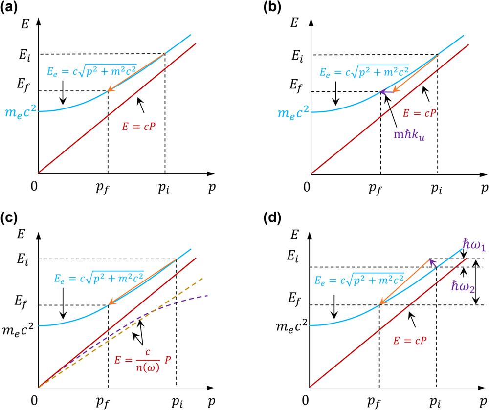
    Fig. 1. The blue solid line represents the electron dispersion curve, while the red dashed line represents the electromagnetic wave dispersion curve. (Ei,pi) and (Ef,pf) represent initial state and final state, respectively. (a) Dispersion relation of a free electron and electromagnetic wave in vacuum; the electromagnetic wave dispersion curve is an asymptote of the electron. (b) Interaction between free electrons and electromagnetic waves in a periodic static magnet environment. (c) Interaction between free electrons and electromagnetic waves in slow-wave structures. Phase velocity of electromagnetic wave is smaller than c. The purple and yellow dashed lines represent the electromagnetic field dispersion curves on a homogeneous medium and hyperbolic dispersive medium, respectively. (d) Compton scattering of a free electron with an electromagnetic field, in which the electron absorbs a photon and emits a high-energy photon.
    (a) Cherenkov radiation, (b) transition radiation, (c) synchrotron radiation, (d) Smith–Purcell effect, (e) undulator radiation, and (f) inverse Compton scattering.
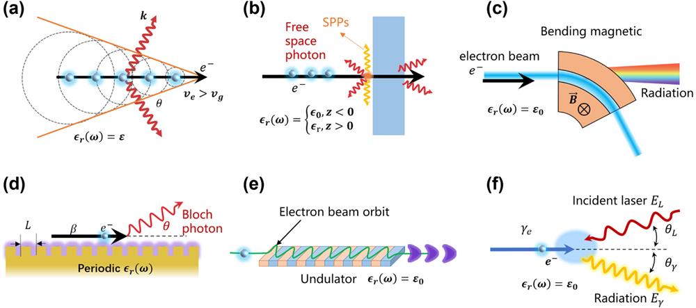
    Fig. 2. (a) Cherenkov radiation, (b) transition radiation, (c) synchrotron radiation, (d) Smith–Purcell effect, (e) undulator radiation, and (f) inverse Compton scattering.
    (a) Schematic diagram of undulator radiation in the SASE regime. Due to the random electrons at the entrance of the undulator, incoherent radiation is emitted, and subsequently the electron beam undergoes density modulation to achieve microbunching on the radiation wavelength scale. With increased coherence, the radiated power along the undulator eventually achieves exponential gain amplification. (b) Illustration of the free-electron trajectory in an undulator and the instantaneously emitted radiation. ψ represents the maximum angle between the electron velocity and the propagation axis, Δθ represents the opening angle of the radiation cone, while λ represents the spatial period of the radiation emitted in the direction of the observation angle θ.
    Fig. 3. (a) Schematic diagram of undulator radiation in the SASE regime. Due to the random electrons at the entrance of the undulator, incoherent radiation is emitted, and subsequently the electron beam undergoes density modulation to achieve microbunching on the radiation wavelength scale. With increased coherence, the radiated power along the undulator eventually achieves exponential gain amplification. (b) Illustration of the free-electron trajectory in an undulator and the instantaneously emitted radiation. ψ represents the maximum angle between the electron velocity and the propagation axis, Δθ represents the opening angle of the radiation cone, while λ represents the spatial period of the radiation emitted in the direction of the observation angle θ.
    (a) Wang et al. experimentally verified LWFA free-electron injection into a conventional static magnetic undulator to achieve SASE-FEL operation in the 27 nm EUV band to achieve exponential gain[95]. (b) SASE-FEL operation in the 830 nm IR band using a compact laser plasma accelerator[114]. (c) LWFA electron-source-driven SASE-FEL at 270 nm with excellent longitudinal coherence for high-gain coherent radiation and amplification at SOLEIL laboratory, France. (d) PWFA electron-source-driven X-ray FEL experimental design.
    Fig. 4. (a) Wang et al. experimentally verified LWFA free-electron injection into a conventional static magnetic undulator to achieve SASE-FEL operation in the 27 nm EUV band to achieve exponential gain[95]. (b) SASE-FEL operation in the 830 nm IR band using a compact laser plasma accelerator[114]. (c) LWFA electron-source-driven SASE-FEL at 270 nm with excellent longitudinal coherence for high-gain coherent radiation and amplification at SOLEIL laboratory, France. (d) PWFA electron-source-driven X-ray FEL experimental design.
    (a) Electric-field-driven micrometer-scale optical undulator fabricated from nanowire arrays excited by ultrashort laser pulses[99]. (b) Femtosecond-laser-driven wire-guided helical undulator for intense terahertz radiation generation[24]. (c) Subwavelength SPPs on a graphene layer serve as the optical undulator, which can modulate the free electrons to emit X-rays even with low-energy electrons[100]. (d) SPP undulator based on multilayer graphene, which could significantly increase the brightness of photons emitted by the undulator[101]. (e) Photon–polariton pair emission in a second-order two-quantum (spontaneous) emission process using a nanophotonic-structure-based undulator[26]. (f) Mating surface paired with graphene in an SPP undulator for producing harmonic emissions[102].
    Fig. 5. (a) Electric-field-driven micrometer-scale optical undulator fabricated from nanowire arrays excited by ultrashort laser pulses[99]. (b) Femtosecond-laser-driven wire-guided helical undulator for intense terahertz radiation generation[24]. (c) Subwavelength SPPs on a graphene layer serve as the optical undulator, which can modulate the free electrons to emit X-rays even with low-energy electrons[100]. (d) SPP undulator based on multilayer graphene, which could significantly increase the brightness of photons emitted by the undulator[101]. (e) Photon–polariton pair emission in a second-order two-quantum (spontaneous) emission process using a nanophotonic-structure-based undulator[26]. (f) Mating surface paired with graphene in an SPP undulator for producing harmonic emissions[102].
    (a) SPP generation and amplification processes, in which the femtosecond-laser-produced electron bunch coherently interacts with the weak seed field it spontaneously emitted in the first stage, resulting in SPP amplification. The color-coded map behind the SPP waveguide represents a close-up view of the SPPs. (b) Feynman diagram depicts the seed formation (stage I) and stimulated amplification (stage II) processes: a first-order spontaneous emission followed by a higher-order process in which the ultrashort bunch length can result in stimulated radiation emission within the instantaneous SPP field[36]. (c) Snapshot showing the electron pulse envelope (black solid line) inside the Ez component of the THz SPPs. The red (blue) area of the field indicates the Ez is in the positive (negative) direction. (d) Simulated electron phase dependence on the THz SPP field in a rest coordinate of the SPP field. It is noted that the space and phase variables in (a) and (b) can be used equivalently via φ=2π(z−vpτd)/λ, where λ is the wavelength of THz SPPs and vp is the phase velocity of the THz SPPs. The orange and blue sections of the curve represent, respectively, the deceleration/acceleration phase of the THz SPPs (a.u., arbitrary units).
    Fig. 6. (a) SPP generation and amplification processes, in which the femtosecond-laser-produced electron bunch coherently interacts with the weak seed field it spontaneously emitted in the first stage, resulting in SPP amplification. The color-coded map behind the SPP waveguide represents a close-up view of the SPPs. (b) Feynman diagram depicts the seed formation (stage I) and stimulated amplification (stage II) processes: a first-order spontaneous emission followed by a higher-order process in which the ultrashort bunch length can result in stimulated radiation emission within the instantaneous SPP field[36]. (c) Snapshot showing the electron pulse envelope (black solid line) inside the Ez component of the THz SPPs. The red (blue) area of the field indicates the Ez is in the positive (negative) direction. (d) Simulated electron phase dependence on the THz SPP field in a rest coordinate of the SPP field. It is noted that the space and phase variables in (a) and (b) can be used equivalently via φ=2π(zvpτd)/λ, where λ is the wavelength of THz SPPs and vp is the phase velocity of the THz SPPs. The orange and blue sections of the curve represent, respectively, the deceleration/acceleration phase of the THz SPPs (a.u., arbitrary units).
    SPP energy amplification by free-electron pumping at the waveguide surface presents a high-gain free-electron laser gain pattern, which undergoes superradiant radiation, exponential gain, and gain saturation owing to dephasing between electron and SPP wave packets.
    Fig. 7. SPP energy amplification by free-electron pumping at the waveguide surface presents a high-gain free-electron laser gain pattern, which undergoes superradiant radiation, exponential gain, and gain saturation owing to dephasing between electron and SPP wave packets.
    (a) Schematic diagram of the betatron radiation driven by laser plasmonic bubbles. (b) Laser-driven plasma undulator that produces coherent synchrotron radiation. The laser plasma functions as both an accelerator and a wiggler[145]. (c) Simulation of controlling free electrons realizing micro bunching (red) in plasma wakefield (green)[150]. (d) Controlling the temporal laser pulse shapes in a bubble-enhanced betatron radiation system to achieve longer oscillation periods[151]. (e) Generation of X-rays with controllable polarization in the betatron regime. Using ionization-induced injection, the radiation-emitting orbits of relativistic electrons are controllable and reproducible with a lower divergence angle[152]. (f) Betatron radiation optimization through artificial Bayesian algorithm[153].
    Fig. 8. (a) Schematic diagram of the betatron radiation driven by laser plasmonic bubbles. (b) Laser-driven plasma undulator that produces coherent synchrotron radiation. The laser plasma functions as both an accelerator and a wiggler[145]. (c) Simulation of controlling free electrons realizing micro bunching (red) in plasma wakefield (green)[150]. (d) Controlling the temporal laser pulse shapes in a bubble-enhanced betatron radiation system to achieve longer oscillation periods[151]. (e) Generation of X-rays with controllable polarization in the betatron regime. Using ionization-induced injection, the radiation-emitting orbits of relativistic electrons are controllable and reproducible with a lower divergence angle[152]. (f) Betatron radiation optimization through artificial Bayesian algorithm[153].
    (a) Schematic representation of ICS. (b) Feynman diagram of ICS.
    Fig. 9. (a) Schematic representation of ICS. (b) Feynman diagram of ICS.
    (a) Miniaturized X-ray source for ICS based on a linear accelerator, proposed by MIT in 2009[172]. (b) All-optical undulator based on ICS configuration[174]. (c) Laser-driven highly confined plasmon modes to modulate electron radiation for demonstrating an equivalent strong-field effect of nonlinear Compton scattering. The electron converts multiple driving photons into a single plasmon. Reprinted with permission from Ref. [177]. Copyright 2019, American Physical Society. (d) Interaction of an FEL with the graphene surface light field can also be compared to an ICS process in which identical harmonic generation occurs[176].
    Fig. 10. (a) Miniaturized X-ray source for ICS based on a linear accelerator, proposed by MIT in 2009[172]. (b) All-optical undulator based on ICS configuration[174]. (c) Laser-driven highly confined plasmon modes to modulate electron radiation for demonstrating an equivalent strong-field effect of nonlinear Compton scattering. The electron converts multiple driving photons into a single plasmon. Reprinted with permission from Ref. [177]. Copyright 2019, American Physical Society. (d) Interaction of an FEL with the graphene surface light field can also be compared to an ICS process in which identical harmonic generation occurs[176].
    (a) Free electrons interact with the vdW material and undergo atomic-level undulator modulation to achieve high-energy X-ray coherent emission[28]. (b) On-chip 1D, all-silicon nanograting Smith–Purcell radiation light source with, for instance, (gated) silicon field emitter arrays[79]. (c) On-chip hyperbolic phonon polarization excited by electrons[124]. (d) High-phase-matched Smith–Purcell emission with optical flatband structure in the meta-surface structure plane[180]. (e) Proposed conceptual scheme and theoretical calculation of the gain curve of the multi-cycle SPP seeded FEL experiment.
    Fig. 11. (a) Free electrons interact with the vdW material and undergo atomic-level undulator modulation to achieve high-energy X-ray coherent emission[28]. (b) On-chip 1D, all-silicon nanograting Smith–Purcell radiation light source with, for instance, (gated) silicon field emitter arrays[79]. (c) On-chip hyperbolic phonon polarization excited by electrons[124]. (d) High-phase-matched Smith–Purcell emission with optical flatband structure in the meta-surface structure plane[180]. (e) Proposed conceptual scheme and theoretical calculation of the gain curve of the multi-cycle SPP seeded FEL experiment.
    (a) As an intense laser pulse is reflected on the plasma mirror, it expels electrons at several narrow specific phase windows of the field. These sub-cycle attosecond electron pulses then experience an integrated momentum kick as they surf the laser electric field (laser streaking) and form periodic fringes in the far field. How the attosecond electron bunches are pulled out from the plasma surface at each optical cycle and form a sharp density peak is illustrated[184]. (b) The attosecond electron bunches are pulled out from the plasma surface at each optical cycle and form a sharp density peak, where z is the direction along the target surface in the incidence plane, and y represents the normal direction of the target surface. (c) Spatial distributions of the electric field amplitude En (red line) and locked phase electron density (blue line). Reprinted with permission from Ref. [132]. Copyright 2012, American Physical Society. (d) Ultrashort terahertz-driven (red) ultrashort electron emission from a metallic nanotip. 800 nm near-IR (NIR; blue) pulses measure this photocurrent, and spectra are recorded as a function of relative pulse delay[186]. (e) Sub-cycle laser pulse focuses on tungsten nanotips. Field emitting attosecond electron pulses are recorded by a time-of-flight spectrometer[185]. (f) Laser-driven carbon nanotube field emission of ultrashort electron pulses[183].
    Fig. 12. (a) As an intense laser pulse is reflected on the plasma mirror, it expels electrons at several narrow specific phase windows of the field. These sub-cycle attosecond electron pulses then experience an integrated momentum kick as they surf the laser electric field (laser streaking) and form periodic fringes in the far field. How the attosecond electron bunches are pulled out from the plasma surface at each optical cycle and form a sharp density peak is illustrated[184]. (b) The attosecond electron bunches are pulled out from the plasma surface at each optical cycle and form a sharp density peak, where z is the direction along the target surface in the incidence plane, and y represents the normal direction of the target surface. (c) Spatial distributions of the electric field amplitude En (red line) and locked phase electron density (blue line). Reprinted with permission from Ref. [132]. Copyright 2012, American Physical Society. (d) Ultrashort terahertz-driven (red) ultrashort electron emission from a metallic nanotip. 800 nm near-IR (NIR; blue) pulses measure this photocurrent, and spectra are recorded as a function of relative pulse delay[186]. (e) Sub-cycle laser pulse focuses on tungsten nanotips. Field emitting attosecond electron pulses are recorded by a time-of-flight spectrometer[185]. (f) Laser-driven carbon nanotube field emission of ultrashort electron pulses[183].
    (a) Attosecond streaking of free-electron pulses at 25 keV. A laser pulse (red) and an electron pulse (blue) intersect at an ultrathin metal mirror (gold), which is penetrable with the electrons. The noncollinear geometry provides laser fields in forward and backward directions along the electron trajectory (red). The transition of the electrons out of the field occurs within 200 as, which is less than half an optical cycle[191]. (b) Optical standing wave structure in the THz band for sub-cycle compression and streaking of free-electron pulses. SHG, second harmonic generation; THz, terahertz source. Reprinted with permission from Ref. [192]. Copyright 2016, The American Association for the Advancement of Science. (c) The energy of sub-relativistic electrons is strongly modulated on the few-femtosecond time scale via the interaction with a traveling wave created in vacuum by two colliding laser pulses at different frequencies. The ponderomotive potential of the optical standing wave can serve the attosecond ballistic bunching of electrons. vg and ve represent traveling wave group velocity and electron velocity, respectively[194]. (d) Concept of the generation of the attosecond electron pulse train via the interaction of electrons with the first optical traveling wave and its characterization via the detection of electron spectra as a function of the relative phase Δϕtw between the first and second traveling waves, separated by a drift distance d. Four infrared pulses (ω1(1), ω2(1), ω1(2), ω2(2)) with controlled relative time delays for the generation of the two phase-locked optical traveling waves. Reprinted with permission from Ref. [195]. Copyright 2018, American Physical Society.
    Fig. 13. (a) Attosecond streaking of free-electron pulses at 25 keV. A laser pulse (red) and an electron pulse (blue) intersect at an ultrathin metal mirror (gold), which is penetrable with the electrons. The noncollinear geometry provides laser fields in forward and backward directions along the electron trajectory (red). The transition of the electrons out of the field occurs within 200 as, which is less than half an optical cycle[191]. (b) Optical standing wave structure in the THz band for sub-cycle compression and streaking of free-electron pulses. SHG, second harmonic generation; THz, terahertz source. Reprinted with permission from Ref. [192]. Copyright 2016, The American Association for the Advancement of Science. (c) The energy of sub-relativistic electrons is strongly modulated on the few-femtosecond time scale via the interaction with a traveling wave created in vacuum by two colliding laser pulses at different frequencies. The ponderomotive potential of the optical standing wave can serve the attosecond ballistic bunching of electrons. vg and ve represent traveling wave group velocity and electron velocity, respectively[194]. (d) Concept of the generation of the attosecond electron pulse train via the interaction of electrons with the first optical traveling wave and its characterization via the detection of electron spectra as a function of the relative phase Δϕtw between the first and second traveling waves, separated by a drift distance d. Four infrared pulses (ω1(1), ω2(1), ω1(2), ω2(2)) with controlled relative time delays for the generation of the two phase-locked optical traveling waves. Reprinted with permission from Ref. [195]. Copyright 2018, American Physical Society.
    Dongdong Zhang, Yushan Zeng, Ye Tian, Ruxin Li. Coherent free-electron light sources[J]. Photonics Insights, 2023, 2(3): R07
    Download Citation