Abstract
Angle tolerant transmissive subtractive color filters incorporating a metasurface exploiting hydrogenated amorphous silicon nanopillars (NPs) on a glass substrate were proposed and demonstrated. The achieved transmission efficiency ranged from 75% to 95% at off-resonance wavelengths. For an NP resonator, electric and magnetic-field distributions in conjunction with absorption cross-sections were investigated to confirm a resonant transmission dip, which is primarily governed by the absorption resulting from simultaneous excitation of magnetic and electric dipoles via Mie scattering. The proposed devices exhibit higher angular tolerance and lower crosstalk for the absorption spectra and, therefore, are applicable with photodetectors, image sensors, and imaging/display devices.Nano structural color filters play a key role in diverse applications, such as imaging devices, ultra-fast displays, solar cells, photodetectors, sensing, and security tags[1–4]. Such structural filters are regarded as a promising substitute to conventional colorant dye/pigment-based filters, which have various disadvantages such as hazardous impact on the environment, performance degradation caused by moisture and ultra-violet irradiation, lower reproduction fidelity, and minimum sustainability. Numerous artificially engineered nanophotonic devices drawing upon multilayered nanostructures and diffraction gratings are invited to manipulate the spectral transmission, reflection, and absorption in the visible spectral band. Although many interesting thin-film structures as in the case of a Fabry–Perot resonator are suggested for ameliorating the color gamut and vivid color saturation, their production is costly. In particular, it is substantially difficult to precisely control the thickness for generating colors at a small scale using the precision lithography process[5–8]. Recently, disordered plasmonic and mesoporous network metamaterials are suggested in the reflection mode[9,10], yet there has been little investigation for the transmission mode. The angular dependence for diffraction gratings is rarely reasonable on the account of the spectral resonance dependent on periodicity[11–13], thereby limiting their use in imaging devices. Moreover, the crosstalk resulting from multiple resonances is accountable for degraded color fidelity.
As an outstanding alternative platform to common multilayered nanostructures, diffractive optical elements, and network metamaterials, metasurfaces, which are referred to as an ultra-thin planar structure that is comprised of finely arranged resonant elements of plasmonic and high-index dielectric nanostructures, have been extensively explored as eminent candidates for building color filtering devices[9–21]. Metasurface-based devices are able to tailor the amplitude, phase, and polarization of light, while they can be efficiently produced using nanofabrication technologies. Highly saturated colors are achievable in plasmonic structures via diffraction[12,13,22], yet attempts to preserve high resolution and guarantee angular independence result in poor color saturation. The use of precious noble metals, such as gold and silver, adversely affects the production cost and prohibits the compatibility with complementary metal–oxide–semiconductor (CMOS) nanofabrication technology. Although aluminum metal is CMOS compatible, it is reported to cause a relatively broad resonance, exhibiting a gamut less saturated than that of silver[23]. Plasmonic devices are susceptible to intrinsic loss in the visible regime to cause excessive power consumption, which deteriorates the transmission performance with respect to the spectral shape, bandwidth, and efficiency. As a result, the color gamut and color saturation become inevitably degraded[2,3,23]. Meanwhile, silicon (Si), the second most ample element in the Earth’s crust, is the backbone of modern technology for nanostructured devices owing to its reliability, cost effectiveness, relatively low intrinsic loss compared to metals, and CMOS compatibility. Nanoresonators in Si, rendering high-index contrast, permit the excitation of the magnetic dipole (MD) resonance as well as the electric dipole (ED) one, which are mediated by Mie scattering[15–20,24]. Si devices have been exploited in embodying functional dielectric metasurfaces[17,18], color filters[15,24–27], antireflection coatings[28], chirality beam splitters[29], and optical holograms[30]. Hydrogenated amorphous Si (a-Si:H) is frequently adopted to create highly efficient, eco-friendly color filters in the transmissive mode[15,25], allowing for industrial-scale deposition at low temperatures on various substrates such as dielectric, glass, plastic, and metal. Moreover, various color filters schemes have been demonstrated in the reflective mode filters utilizing photonic crystals[31–34], Si structures[35–42], low index materials of titania[43], and SiGe resonators[44]. Despite tremendous advances in a number of previous strategies in realizing the color in the reflection mode, the investigation of subtractive coloration, which exhibits a high angle tolerance in the transmissive mode, has not been reported for a-Si:H structures of a high aspect ratio. The adoption of a higher aspect ratio of a-Si:H structures is anticipated to help increase the absorption, while the resonance modes can be absolutely claimed for different angles of incidence to facilitate Mie scattering.
In this study, we propose highly angle tolerant subtractive color filters that capitalize on an all-dielectric metasurface using a-Si:H nanopillars (NPs) with a high aspect ratio, featuring enhanced transmission ranging from 75% to 95%, in tandem with a broad bandwidth translating into a wider color gamut. Three primary subtractive colors of cyan, magenta, and yellow (CMY) were manufactured to deliver enhanced color saturation. The color tunability related to the a-Si:H metasurface, which features the transmission spectra with a resonance dip, were judiciously investigated in terms of the NP diameter, so that a broad range of color images could be achieved. The near-field electric (E-) and magnetic (H-) field profiles in combination with the absorption and scattering cross-sections were examined for the NP. The mechanism underpinning the transmission dip is supported by absorption through the existence of dominant MD over ED resonances. A high-resolution microscale colored letter pattern was created by appropriately tailoring the NP diameter, thereby proving flexible and efficient colorations. The low crosstalk for absorption was explored as well. The proposed devices have the potential to be implemented in high-quality CMOS image sensors, photodetectors, and display devices.
Sign up for Chinese Optics Letters TOC. Get the latest issue of Chinese Optics Letters delivered right to you!Sign up now
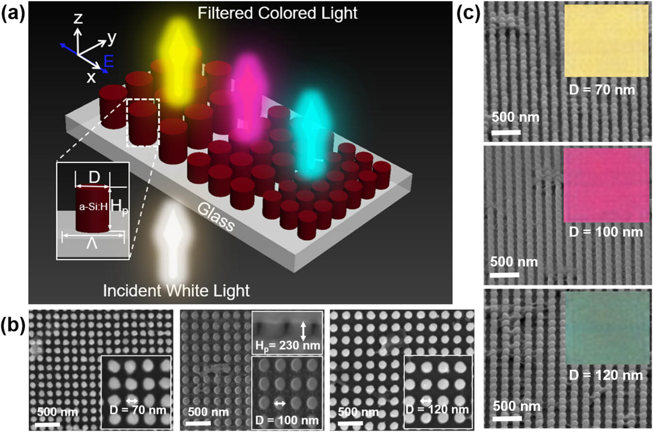
Figure 1(a) shows the schematic configuration of the proposed color filters that rely on a dielectric metasurface, which is composed of an array of a-Si:H NPs with 230 nm thickness () residing on a slide glass. The filling ratio of the NP, defined as the ratio of the diameter () of the NP to period (), is fixed at 0.5. The aspect ratio () is engineered to enhance the transmission at off-resonance and obtain a resonance dip with a broader bandwidth, enabling a wider color gamut. For incident light, transverse electric (TE) polarization is indicated by the ‘E-field’, which is aligned along the direction, as illustrated in Fig. 1(a). For the transverse magnetic (TM) polarization, the E-field is presumed to be aligned along the direction. Incident white light is selectively blocked at the resonance wavelength to produce specific colors, depending on the structural parameters associated with the NP. For an a-Si:H film deposited through chemical vapor deposition at a low temperature of 250°C, the refractive index is measured and plotted as given in Appendix A. The scanning electron microscope (SEM) images of the prepared filters with diameters of , 100, and 120 nm are shown in Figs. 1(b) and 1(c). The insets in Fig. 1(b) show the zoomed SEM and focused ion beam (FIB) images depicting the cross-section of the magenta filter. Insets in Fig. 1(c) for the tilt view reveal the captured images related to CMY colors.

Figure 1.(a) Schematic of the proposed color filters incorporating a-Si:H NPs. Incident white light is filtered into three primary subtractive colors of CMY. (b) Top view and (c) tilt view of SEM images for the three primary subtractive color filters for CMY with diameters of , 100, and 120 nm, respectively. For the magenta filter, inset in (b) on top right of the SEM image includes the FIB cross-section image depicting the height of the a-Si:H NP. Inset in (c) for the tilt view shows the captured colored images.
Figure 2(a) illustrates the transmission spectral response for the filters, exhibiting a resonance dip corresponding to the primary colors of CMY. In an attempt to evaluate the devices, the color responses are accordingly mapped in the International Commission on Illumination (CIE) 1931 chromaticity diagram, which is shown in Fig. 2(b). The filters lead to transmission efficiencies ranging from 75% to 95% at off-resonance wavelengths in conjunction with the resonance dip, leading to a wider color gamut and higher color saturation. The irregular mismatch between the simulated and measured transmission spectra is ascribed to the unexpected structural asymmetries in combination with the surface and sidewall roughness of the NPs, which might be incurred by fabrication inaccuracies and variations in the material deposition.
Figure 2.(a) Measured and calculated transmission spectra for the subtractive color filters with diameters of , 100, and 120 nm. (b) Color responses corresponding to the transmission spectra in (a) mapped in the CIE 1931 chromaticity diagram.
As shown in Fig. 3(a), the simulated and measured transmission spectra for the a-Si:H metasurface are plotted alongside the resonance dip, with the NP diameter varying from 60 to 130 nm in 10 nm intervals. The black dashed line traces the position of the resonance dip, indicating a trend of red shift. The transmission resonance dip occurs owing to the presence of MD and ED via Mie scattering. The insets in Fig. 3(a)(ii) depict the vivid color images for the fabricated filters employing NPs of different diameters. Figure 3(b) shows the corresponding color matching coordinates in the CIE 1931 chromaticity diagram, on top of the spectra for the transmission resonance from Fig. 3(a) for both simulated and measured cases. There is a good agreement between the captured color images and the corresponding CIE color map, which is indicative of enhanced color fidelity.
Figure 3.(a) (i) Simulated and (ii) measured transmission spectra for the color filter when the NP diameter is varied from 60 to 130 nm in increments of 10 nm. (b) Color responses corresponding to the transmission spectra in (a) are mapped in the CIE 1931 chromaticity diagram. Insets in (a)(ii) show the captured vivid color images.
A nanostructured resonator that engages high-index materials such as Si allows for the excitation of MD and ED modes via Mie scattering[15–20,24]. In an effort to unequivocally understand the mechanism underlying the wavelength-selective transmission dip in connection with the metasurface resorting to a lattice of a-Si:H NPs, we examined the E- and H-field profiles at the resonance wavelength as well as the absorption cross-section for the NP. Each dielectric NP resonator is analogous to a truncated waveguide, the effective refractive indices of which are dependent upon the diameter[45], serving as a Fabry–Perot etalon featuring a low-quality factor.
Figure 4(a) shows the calculated transmission, reflection, and absorption spectra for the filter with an NP diameter of . The device provides a dip for transmission, zero reflection, and high absorption at the resonance wavelength. The calculated absorption, scattering, and extinction cross-sections for the NP are displayed in Fig. 4(b), where the peak of the absorption cross-section is concurrent with the resonance dip in the transmission or the absorption peak, supporting the hypothesis that absorption cross-sections dictate spectral transmission. The position of the MD and ED resonances is marked on the spectra associated with the absorption cross-section. Figures 4(c) through 4(f) delineate the field profiles pertaining to the resonant MD and ED modes initiated by the absorption cross-sections. The dominant MD monitored at the wavelength of 565 nm is indicated by the reinforced H-field, as observed in Fig. 4(d), alongside the circular displacement current in connection with the E-field shown in the vector plot in Fig. 4(c), on the xz cross-section that cuts through the center of the a-Si:H NP. The enhanced E-field is thought to represent the ED mode at the same resonance wavelength as shown in Fig. 4(e), as in the case of the MD mode, in combination with the current loop of the H-field, which is shown in the vector plot in Fig. 4(f), on the yz cross-section that cuts through the center of the a-Si:H NP. The black dashed line represents the interface between the two different media. The low refractive index contrast at the ends of the truncated waveguide leads to the broad resonance in the transmission spectra, which can be considered leakage of confined light into the substrate. Moreover, the significantly broad resonance is anticipated to occur due to the geometrical irregularities in NPs. The MD and ED excitations are better distinguished under different aspect and filling ratios[15–17]. The simultaneous excitation of the MD and ED and their mutual interactions can be attributed to Kerker scattering[46]. A strong MD is induced when the wavelength inside the nanostructure becomes proportional to its dimension under the condition of , where is the refractive index, is the radius, and is the wavelength. A subwavelength nanoparticle () requires a large index of refraction to facilitate such resonance[47].
Figure 4.(a) Simulated transmission (T), reflection (R), and absorption (A) spectra, denoted by the arrow, for a typical filter with . (b) Calculated cross-sections pertaining to the peak absorption (denoted by the arrow), scattering, and extinction, where (c) E-field and (d) H-field profiles are superimposed on the vector plot for the MD, and (e) E-field and (f) H-field profiles are superimposed on the vector plot for the ED at the resonance wavelength of 565 nm for the filter with .
The transmission spectra were assessed with respect to the various incident angles for the TE and TM polarizations. Figures 5(a) and 5(b) show ‘simulated’ transmission spectra with respect to the incident angle for TE and TM polarizations, while Figs. 5(c) and 5(d) present ‘measured’ transmission spectra for both polarizations. The transmission resonance dip was preserved, indicating a relaxed angular tolerance for angles ranging up to about 45° and 40° for the TE and TM polarization, respectively, for both simulated and measured cases, which are in decent agreement. It was observed via simulations that the filters exhibit noticeable degradations in the spectral performance for incident angles beyond 45° and 40° for the TE and TM polarization, respectively. A resonance mode can be categorically claimed for the NPs for different incidence angles for two polarizations, as in the case of normal incidence, implying that the structure of concern can efficiently facilitate Mie scattering to render the relaxed angular tolerance as desired[48]. The discrepancy between the simulation and experiment results, particularly in the spectral band ranging from 650 to 700 nm, is thought to stem from degraded efficiencies of the measurement system for larger angles of incidence. In view of their enhanced angular tolerance, polarization independence, and reduced crosstalk, the proposed filters can be readily applied to photodetectors and image sensors.
Figure 5.Contour plot of the transmission spectra in terms of the varied angles of incidence: (a), (b) ‘simulated’ and (c), (d) ‘measured’ cases for the TE and TM polarizations for a filter with .
The transmission/reflection spectra, absorption, scattering cross-sections, and field profiles for the proposed devices were examined with the assistance of a simulation tool based on the finite difference time domain (FDTD) method (FDTD Solutions, Lumerical Inc., Canada)[49]. A normally incident plane wave in the visible band illuminated a unit cell with a periodic boundary condition to model an array of a-Si:H NPs. The dispersion characteristics of a-Si:H in the visible band, which was observed through a reflecto-spectrometer (Filmtek4000, SCI), were considered in the simulations. The dispersion characteristics of , which are used for the simulations, were derived from the multi-coefficient model supplied by the simulation tool[49].
The cell constituting the proposed color filters was designed and created with dimensions of . For the fabrication of the a-Si:H metasurface, a 230 nm thick a-Si:H film was deposited on a glass substrate through a gas mixture of silane (SiH4) and helium (He) carrier using plasma enhanced chemical vapor deposition (Oxford, Plasmalab System 100)[50]. After spin coating of an electron (e-) beam resist (ZEP520A from Zeon Chemicals), a thin layer of e-spacer 300Z (Showa Denko) was applied to avoid charging during subsequent e-beam exposure. The pattern was then formed using e-beam writing (EBL, Raith150) and subsequent development in ZED-N50. A 50 nm thick aluminum layer was then deposited by e-beam evaporation (Temescal BJD-2000), followed by a lift-off process by soaking the sample in the resist remover (ZDMAC from ZEON Co.). The remaining aluminum pattern array was used as an etch mask to transfer the designed pattern to the a-Si:H film using fluorine-based inductively coupled plasma-reactive ion etching (Oxford Plasmalab System 100). The etching conditions were optimized to attain a highly anisotropic etching profile for the a-Si:H. The residual aluminum etch mask was eventually removed using a wet etching solution.
The fabricated a-Si:H pattern was visually inspected by dual beam (SEM/FIB) high-resolution SEM (FIB II, Quanta 3D FEG, FEI). The transmission spectra were monitored by launching a collimated beam from a halogen lamp (HL-2000-FHSA, Ocean Optics), which was polarized through a calcite crystal polarizer (GTH 10M-A, Thorlabs), to the prepared color filter mounted on a motorized rotation stage. The optical output was captured by spectrometry (Avaspec-3648, Avantes) using a multimode fiber. Images for each color were taken via digital microscopy (Leica DM4000 M). The beam size was controlled by a pinhole, resulting in the size of the beam being smaller than that of the sample. The calibration was carried out by taking the reference of the source light intensity in the absence of the filter, and the dark reference was taken without the illuminance of the source light. The measured transmission spectra as a function of the incident angle were fulfilled through an angle-resolved micro-spectroscopy system (ARM, Ideaoptics, China).
Subtractive color filters based on an all-dielectric metasurface, with a high aspect ratio of a-Si:H NPs on a glass substrate, were realized to yield high angular tolerance ranging up to 45° and transmission efficiencies up to 95% at longer off-resonance wavelengths. A suite of filters with different NP diameters were manufactured to demonstrate a broad range of color tuning in the visible band, providing a wider color gamut and vivid color saturation. The resonant transmission dip was accounted for by the absorption resulting from the dominant excitation of the MD rather than the ED mediated by Mie scattering, which was elucidated with the help of the near-field profiles of the E- and H-fields. The transmission spectra were dictated by absorption cross-sections. In future research, metasurface devices will be further explored to interpret the interactions between the MD and ED modes, which can be implemented in various applications, such as optical nanoantennas, beam steering, and beam focusing. The proposed devices will be available for application, including photodetectors, image sensors, color displays, and imaging.
References
[1] H. Kim, J. Ge, J. Kim, S. E. Choi, H. Lee, H. Lee, W. Park, Y. Yin, S. Kwon. Nat. Photon., 3, 534(2009).
[2] T. Xu, Y.-K. Wu, X. Luo, L. J. Guo. Nat. Commun., 1, 59(2010).
[3] A. S. Roberts, A. Pors, O. Albrektsen, S. I. Bozhevolnyi. Nano Lett., 14, 783(2014).
[4] J. Y. Lee, K. T. Lee, S. Seo, L. J. Guo. Sci. Rep., 4, 4192(2014).
[5] C. Ji, K. T. Lee, L. J. Guo. Opt. Lett., 44, 86(2019).
[6] J. Boroumand, S. Das, A. Vázquez-Guardado, D. Franklin, D. Chanda. Sci. Rep., 6, 31013(2016).
[7] K. T. Lee, S. Y. Han, H. J. Park. Adv. Opt. Mater., 5(2017).
[8] C. S. Park, V. R. Shrestha, S. S. Lee, E. S. Kim, D. Y. Choi. Sci. Rep., 5, 8467(2015).
[9] H. Galinski, G. Favraud, H. Dong, J. S. T. Gongora, G. Favaro, M. Döbeli, R. Spolenak, A. Fratalocchi, F. Capasso. Light Sci. Appl., 6, e16233(2017).
[10] A. Ruiz-Clavijo, Y. Tsurimaki, O. Caballero-Calero, G. Ni, G. Chen, S. V. Boriskina, M. Martín-González. ACS Photon., 5, 2120(2018).
[11] A. Kristensen, J. K. W. Yang, S. I. Bozhevolnyi, S. Link, P. Nordlander, N. J. Halas, N. A. Mortensen. Nat. Rev. Mater., 2, 16088(2016).
[12] J. Wang, Q. Fan, S. Zhang, Z. Zhang, H. Zhang, Y. Liang, X. Cao, T. Xu. Appl. Phys. Lett., 110, 031110(2017).
[13] V. R. Shrestha, S. S. Lee, E. S. Kim, D. Y. Choi. Nano Lett., 14, 6672(2014).
[14] D. Lin, P. Fan, E. Hasman, M. L. Brongersma. Science, 345, 298(2014).
[15] C. S. Park, V. R. Shrestha, W. Yue, S. Gao, S. S. Lee, E. S. Kim, D. Y. Choi. Sci. Rep., 7, 2556(2017).
[16] J. Xiang, J. Li, Z. Zhou, S. Jiang, J. Chen, Q. Dai, S. Tie, S. Lan, X. Wang. Laser Photon. Rev., 12, 1800032(2018).
[17] I. Staude, A. E. Miroshnichenko, M. Decker, N. T. Fofang, S. Liu, E. Gonzales, J. Dominguez, T. S. Luk, D. N. Neshev, I. Brener, Y. Kivshar. ACS Nano, 7, 7824(2013).
[18] M. Decker, I. Staude, M. Falkner, J. Dominguez, D. N. Neshev, I. Brener, T. Pertsch, Y. S. Kivshar. Adv. Opt. Mater., 3, 813(2015).
[19] A. I. Kuznetsov, A. E. Miroshnichenko, M. L. Brongersma, Y. S. Kivshar, B. Luk’yanchuk. Science, 354, aag2472(2016).
[20] C. Y. Yang, J. H. Yang, Z. Y. Yang, Z. X. Zhou, M. G. Sun, V. E. Babicheva, K. P. Chen. ACS Photon., 5, 2596(2018).
[21] T. Hu, C. K. Tseng, Y. H. Fu, Z. Xu, Y. Dong, S. Wang, K. H. Lai, V. Bliznetsov, S. Zhu, Q. Lin, Y. Gu. Opt. Express, 26, 19548(2018).
[22] H. Lochbihler. Opt. Express, 17, 12189(2009).
[23] S. J. Tan, L. Zhang, D. Zhu, X. M. Goh, Y. M. Wang, K. Kumar, C. W. Qiu, J. K. W. Yang. Nano Lett., 14, 4023(2014).
[24] W. Yue, S. Gao, S. S. Lee, E. S. Kim, D. Y. Choi. Laser Photon. Rev., 11, 1600285(2017).
[25] I. Koirala, V. R. Shrestha, C. S. Park, S. Gao, S. S. Lee, D. Y. Choi. Sci. Rep., 7, 13574(2017).
[26] J. Proust, F. Bedu, B. Gallas, I. Ozerov, N. Bonod. ACS Nano, 10, 7761(2016).
[27] Y. Nagasaki, M. Suzuki, J. Takahara. Nano Lett., 17, 7500(2017).
[28] P. Spinelli, M. A. Verschuuren, A. Polman. Nat. Commun., 3, 692(2012).
[29] M. Khorasaninejad, K. B. Crozier. Nat. Commun., 5, 5386(2015).
[30] B. Wang, F. Dong, Q. T. Li, D. Yang, C. Sun, J. Chen, Z. Song, L. Xu, W. Chu, Y. F. Xiao, Q. Gong, Y. Li. Nano Lett., 16, 5235(2016).
[31] A. C. Arsenault, D. P. Puzzo, I. Manners, G. A. Ozin. Nat. Photon., 1, 468(2007).
[32] P. Kang, S. O. Ogunbo, D. Erickson. Langmuir, 27, 9676(2011).
[33] H. S. Lee, T. S. Shim, H. Hwang, S.-M. Yang, S.-H. Kim. Chem. Mater., 25, 2684(2013).
[34] E.-H. Cho, H.-S. Kim, B.-H. Cheong, O. Prudnikov, W. Xianyua, J.-S. Sohn, D.-J. Ma, H.-Y. Choi, N.-C. Park, Y.-P. Park. Opt. Express, 17, 8621(2009).
[35] V. Flauraud, M. Reyes, R. Paniagua-Dominguez, A. I. Kuznetsov, J. Brugger. ACS Photon., 4, 1913(2017).
[36] E. Højlund-Nielsen, J. Weirich, J. Nørregaard, J. Garnaes, N. A. Mortensen, A. Kristensen. J. Nanophoton., 8, 083988(2014).
[37] Y. Nagasaki, M. Suzuki, I. Hotta, J. Takahara. ACS Photon., 5, 1460(2018).
[38] V. Vashistha, G. Vaidya, R. S. Hegde, A. E. Serebryannikov, N. Bonod, M. Krawczyk. ACS Photon., 4, 1076(2017).
[39] B. M. Gawlik, G. Cossio, H. Kwon, Z. Jurado, B. Palacios, S. Singhal, A. Alù, E. T. Yu, S. V. Sreenivasan. Opt. Express, 26, 30952(2018).
[40] Y. Kanamori, T. Ozaki, K. Hane. Opt. Express, 22, 25663(2014).
[41] Z. Dong, J. Ho, Y. F. Yu, Y. H. Fu, R. Paniagua-Dominguez, S. Wang, A. I. Kuznetsov, J. K. W. Yang. Nano Lett., 17, 7620(2017).
[42] K. Seo, M. Wober, P. Steinvurzel, E. Schonbrun, Y. Dan, T. Ellenbogen, K. B. Crozier. Nano Lett., 11, 1851(2011).
[43] S. Sun, Z. Zhou, C. Zhang, Y. Gao, Z. Duan, S. Xiao, Q. Song. ACS Nano, 11, 4445(2017).
[44] T. Wood, M. Naffouti, J. Berthelot, T. David, J.-B. Claude, L. Métayer, A. Delobbe, L. Favre, A. Ronda, I. Berbezier, N. Bonod, M. Abbarchi. ACS Photon., 4, 873(2017).
[45] A. Arbabi, Y. Horie, M. Bagheri, A. Faraon. Nat. Nanotechnol., 10, 937(2015).
[46] Y. H. Fu, A. I. Kuznetsov, A. E. Miroshnichenko, Y. F. Yu, B. Luk’yanchuk. Nat. Commun., 4, 1527(2013).
[47] S. Kruk, Y. Kivshar. ACS Photon., 4, 2638(2017).
[48] P. Moitra, B. A. Slovick, W. Li, I. I. Kravchencko, D. P. Briggs, S. Krishnamurthy, J. Valentine. ACS Photon., 2, 692(2015).
[49] (2019).
[50] X. Gai, D. Y. Choi, B. Luther-Davies. Opt. Express, 22, 9948(2014).