Lijuan YAO, Xuan FANG, Dan FANG, Chenhao GAO, Shengda LIU, Ruxue LI, Dengkui WANG, Zhipeng WEI, Xiaohua WANG. Research Progress of the Stability and Photodetectors Applications of Organic-inorganic Hybrid Halide Perovskite Materials (Invited)[J]. Acta Photonica Sinica, 2021, 50(1): 26
Search by keywords or author
- Acta Photonica Sinica
- Vol. 50, Issue 1, 26 (2021)
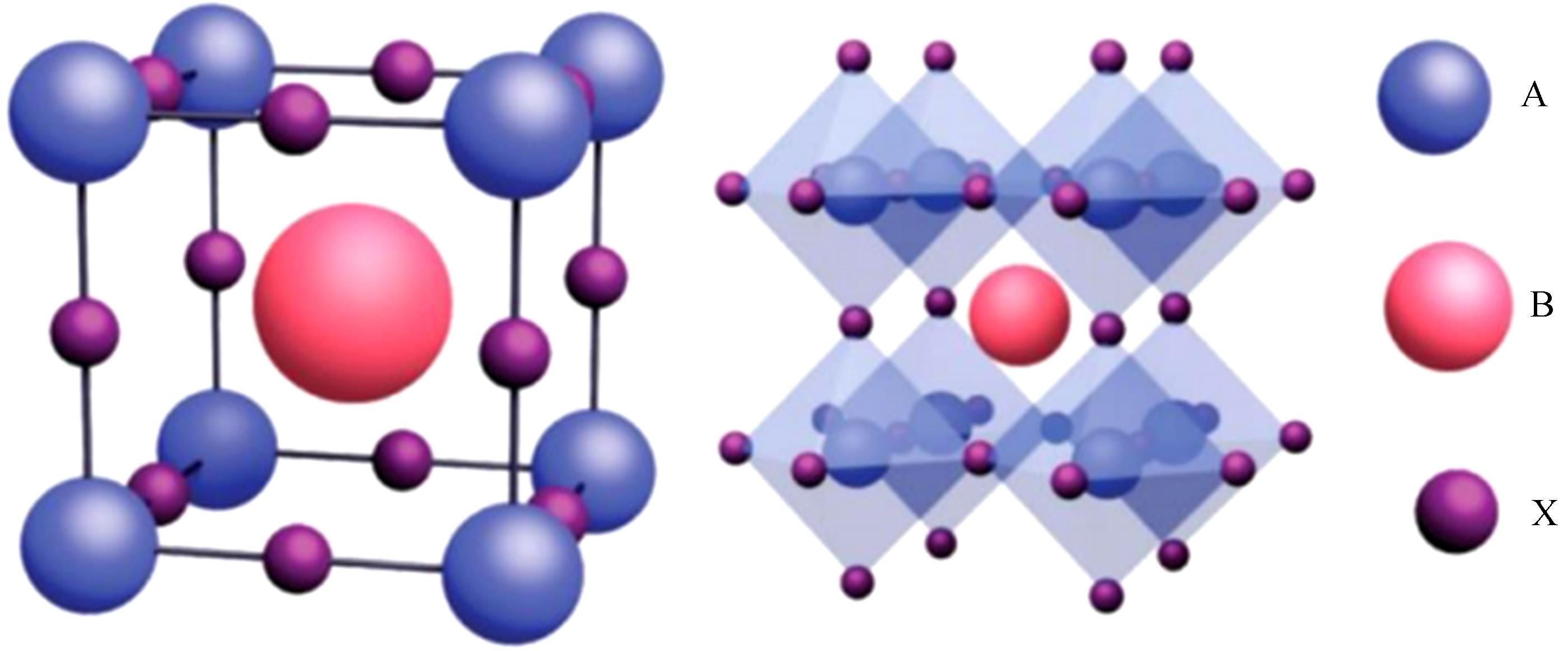
![Unit cell of an ideal cubic perovskite ABX3 (left), and their extended crystalline structured connected by corner-sharing [BX6]4- octahedra (right). Reproduced with permission[5]. Copyright 2016, Wiley-VCH](/richHtml/gzxb/2021/50/1/26/img_1.png)
Fig. 1. Unit cell of an ideal cubic perovskite ABX3 (left), and their extended crystalline structured connected by corner-sharing [BX6]4- octahedra (right). Reproduced with permission[5]. Copyright 2016, Wiley-VCH
![The top layer atoms and simulated STM images[33]. Copyright 2017, American Chemical Society](/richHtml/gzxb/2021/50/1/26/img_2.png)
Fig. 2. The top layer atoms and simulated STM images[33]. Copyright 2017, American Chemical Society
Fig. 3. TGA curve of CH3NH3PbI3 decomposition[48]. Copyright 2014, American Chemical Society
Fig. 4. The PL image of a large number of samples of MAPbI3 excited by a commercial color camera at 458 nm before degradation, in which the pure MAPbI3 structure is seen as red (left image); the right image is another image of the same area after degradation, in which green emission is observed, corresponding Launched on PbI[52]2.Copyright 2016, American Chemical Society
Fig. 5. Synthetic procedure for perovskite nanocrystals[55]. Copyright 2016, Wiley-VCH
Fig. 6. The top-down synthetic method towards methylammonium lead halide perovskite nanocrystals[58]. Copyright 2017, Wiley-VCH
Fig. 7. Schematic of the ABX3 perovskite crystal structure (left); Elements that are used as ions in the mixed-metal perovskite materials (right)[59].Copyright 2017, Royal Society of Chemistry
Fig. 8. Regular (PbI6) octahedral chain in CH3NH3PbI3 (left) and distorted chain in 12.5 at.% Cs-doped CH3NH3PbI3 (right). (Gray/Purple/Brown/Blue/Pink/Turquoise sphere represents Pb/I/C/N/H/Cs atom)[66]
Fig. 9. Schematic overview of contraction of octahedral after partially replacing Pb2+ by smaller Zn2+ ions[72]
Fig. 10. The local geometry and the electron localization function (ELF) contour plots of MAPbI3Cl3-x before and after Zn doping[69]. Copyright 2018,Elsevier
Fig. 11. Schematics formation of perovskite layer with and without addition of Ni2+ metal ions, scanning electron microscopy images of PbI2 films with various NiCl2:PbI2 molar ratio, SEM images of corresponding perovskite films[70]. Copyright 2018, Wiley-VCH
Fig. 12. The crystal structure of pristine MAPbI3 (left) and MAPbI3 (Ni) perovskite (right), in which Ni-I and Ni-N bonds are indicated with green lines[70]. Copyright 2018, Wiley-VCH
Fig. 13. Perovskite structures of CH3NH3Pb (SCN)2I (left) and CH3NH3PbI3 (right) for comparison. Carbon gray, iodine red, lead pink, nitrogen blue, sulfur yellow[80]. Copyright 2015, Wiley-VCH
Fig. 14. SEM images of CH3NH3Pb(SCN)x I3-x film prepared using DMF as the solvent of Pb(SCN)2 and pure CH3NH3PbI3 film (right)[79]. Copyright 2019, American Chemical Society
Fig. 15. Schematic device structure of a MAPbI3/UCns bilayer photodetector and scanning electron microscopy and transmission electron microscopy of the neat UCns layer, MAPbI3 arrays and bilayer[56]. Copyright 2017, American Chemical Society
Fig. 16. Detectivity and responsivity as a function of time showing long-term environmental stability for MAPbI3/UCns bilayer and the neat MAPbI3 photodetectors exposure under ambient condition with 30-40% relative humidity (RH)[56]. Copyright 2017, American Chemical Society
Fig. 17. Water soaking showing strong water resistance of the MAPbI3/UCns bilayer in contrast to the neat MAPbI3 film[56]. Copyright 2017, American Chemical Society
Fig. 18. Schematic configuration photodetector and cross-section SEM image of CH3NH3PbI3/C8BTBT heterojunction thin films, and XRD spectra of CH3NH3PbI3 (black) and CH3NH3PbI3/C8BTBT heterojunction (red) thin films[83]. Copyright 2017, Wiley-VCH
Fig. 19. Photocurrent and responsivity of CH3NH3PbI3 and CH3NH3PbI3/C8BTBT heterojunction photodetectors measured in ambient condition for 20 days[83]. Copyright 2017, Wiley-VCH
|

Set citation alerts for the article
Please enter your email address


