Abstract
We demonstrate a high-speed silicon carrier-depletion Michelson interferometric (MI) modulator with a low on-chip insertion loss of 3 dB. The modulator features a compact size of and a static high extinction ratio of . The of the MI modulator is under a reverse bias of to , indicating a high modulation efficiency. Experimental results show that a 4-level pulse amplitude modulation up to 20 Gbaud is achieved with a bit error rate of , and a 30 Gb/s binary phase-shift-keying modulation is realized with an error vector magnitude of 25.8%.Due to the inherent merit of compatibility with mature CMOS technologies, silicon photonics have developed dramatically in recent years. Multiple active and passive devices with excellent performances have been demonstrated such as modulators, photodetectors, switches, splitters, couplers, and polarization rotators, etc.[1–3]. Compared with the III–V semiconductor materials such as InP, the large wafer size and integration capability make silicon-on-insulator (SOI) material more attractive for potential low-cost mass production and photonic-electronic convergence on a single chip.
Among the various silicon photonic devices, silicon modulators are one of the research hotspots, for their broad applications in short-reach data centers and supercomputers[4,5]. Modulation in silicon is typically realized based on carrier injection[6], carrier accumulation[7], or carrier depletion[8] using the free-carrier plasma dispersion effect. There are two types of silicon modulator structures. One is the resonance-based modulator, which features a high modulation speed up to 60 Gb/s, compact size, and a high modulation efficiency[9]. Another one is based on the Mach–Zehnder interferometer (MZI) structure, with a broad optical bandwidth and a high temperature tolerance. The recorded modulation speed is higher than 70 Gb/s[10]. By combining the merits of both MZI and microring resonator structures, a high-speed microring modulator based on coupling modulation has been demonstrated with a low drive voltage and low power consumption[11]. High-order modulation formats have also been realized using silicon modulators that can generate a higher data rate with a higher spectral efficiency. For example, 6.25 Gbaud Nyquist 64-quadrature amplitude modulation (QAM) was generated with a subcarrier multiplexed technique on silicon modulators[12]. 32 Gbaud silicon polarization-division-multiplexed quadrature phase-shift keying (PDM-QPSK) modulators[13] and 28 Gbaud silicon PDM-16-QAM modulators[14] have also been reported recently, with an accumulated data rate up to 200 Gb/s.
The MZI-based modulators (MZMs) usually have long active arms to achieve a certain modulation depth demanded in practical applications. However, the long arm length leads to a high insertion loss (IL) due to the free-carrier absorption (FCA) of the PN junctions. To lower the IL of MZMs, the doping concentrations of the PN junctions should be reduced, but inevitably at the expense of a lower modulation depth. To obtain a high modulation depth without increasing the physical length of active arms, silicon Michelson interferometer (MI)-based modulators (MIMs) have been proposed[15,16]. In the MIMs, the propagating light makes a round trip along the phase-shifting waveguides, and thus the RF signal interacts with both the forward and backward light, resulting in enhanced modulation efficiency as well as a more compact device. It should be noted that because the RF signal is phase mismatched with the backward propagating light, the modulation bandwidth is sacrificed compared to the MZM with a double arm length.
Sign up for Chinese Optics Letters TOC. Get the latest issue of Chinese Optics Letters delivered right to you!Sign up now
In this Letter, we demonstrate a low-loss high extinction ratio (ER) MIM with a single-drive push-pull traveling wave electrode (TWE). The single-drive TWE has an improved modulation bandwidth due to its lower microwave attenuation arising from the reduced capacitance compared to a dual-drive TWE[10,17]. The MIM has a high static ER of more than 30 dB and a low of . 30 Gb/s binary phase-shift keying (BPSK) and 40 Gb/s 4-level pulse amplitude modulation (PAM)-4 modulations have been successfully realized. The on-chip IL is only . The low IL MIM is beneficial in reducing the power budget for on-chip integrated systems in green optical communications and biochemical sensing applications[18]. The back reflection to the light source can be inhibited by using on-chip isolation structures[19].
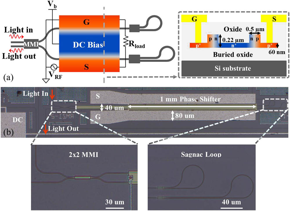
Figure 1(a) shows the schematic structure of the single-drive push-pull MIM, consisting of one 3 dB multimode interferometer (MMI) coupler and two imbalanced modulation arms terminated with two Sagnac loop reflectors. The MMI coupler is 5 μm wide and 29.5 μm long with an IL of . Light is split and combined by the same MMI coupler. Each arm is integrated with a 1 mm long phase shifter based on a lateral PN junction. The two arms have a length difference of 180 μm. The bending radius of the Sagnac loop is 20 μm and the MMI is 3.4 μm wide and 10 μm long.

Figure 1.(a) Schematic of the single-drive push-pull MIM. The inset shows the cross section of the modulation arms. (b) An SEM image of the fabricated MIM. The insets show the zoom-in images of the MMI coupler and the end Sagnac loop reflectors.
The SOI waveguide has a width of 500 nm, a height of 220 nm, and a remained slab height of 60 nm. The active waveguide is embedded with PN junctions with p-type and n-type doping concentrations of and , respectively. The PN junction has an offset of 100 nm from the waveguide center toward the n-doping region in order to maximize the modulation efficiency and meanwhile reduce the FCA loss. The heavily - and -doping concentrations are to ensure good ohmic contact with the metals. The TWE is optimized based on an equivalent circuit model in which the effects of the coplanar strip lines and the PN junctions are both taken into consideration[15]. To achieve a large electro-optical (EO) bandwidth, first, the characteristic impedance of the TWE should be close to 50 Ω to reduce the RF reflections; second, the microwave effective refractive index should match the optical group index to synchronize the RF signal and optical waves; third, the microwave attenuation should be as low as possible. After the PN junction profile is determined for a high modulation efficiency, the bandwidth improvement can be achieved by optimizing the dimensions of the metal lines. Calculated by FEM simulations with COMSOL Multiphysics, we found that the width and the gap separation between the two metal lines are most critical. To balance these parameters for a better EO bandwidth, the 80 μm wide signal (S) and ground (G) metal lines of the TWE are connected to the heavily -doping regions positioned outside the MI arms. The two metal lines have a gap of 40 μm. The DC bias metal line is connected to the -doping region located between the two arms.
The modulator was fabricated on a high-resistivity SOI wafer with a top silicon layer thickness of 220 nm and a buried-oxide layer thickness of 2 μm using CMOS compatible processes. Figure 1(b) shows a scanning electron microscope (SEM) image of the fabricated MIM. Only one RF input signal () was used to drive the two PN junctions connected back to back. The bias voltage () was used to keep the PN junctions reversely biased, making the voltages applied onto the two PN junctions swing between . A push-pull drive thus resulted. The fabrication details can be found in our previous work[8,11].
We first measured the transmission spectra of the MIM by using a Santec Swept Test System (Santec TLS-710). The input laser light was set to TE polarization. Tapered-lensed fibers were used for light input and output coupling. Figure 2(a) shows the measured transmission spectra normalized to a test waveguide. The reverse bias was applied to the shorter arm of the MIM. The total fiber-to-fiber IL is 8 dB, including on-chip IL and input/output coupling loss. The on-chip IL is much lower than the values reported in the previous MIMs[15,16]. The free spectral range (FSR) of the interference fringe is 3.22 nm and the static ER exceeds 30 dB. The high ER is one of the intrinsic merits of the MI. As light split and recombination are enabled by the same MMI coupler, the MI has a much higher tolerance to an uneven splitting ratio of the coupler compared to an MZI. Figure 2(b) shows the extracted phase shift as a function of the bias voltage. As depicted in Refs. [15,16], the phase shift is expressed as , where is the wavelength shift of the spectral notch. It can be observed that the phase shift increases more slowly when the reverse bias becomes larger. As the active arm is lightly doped and is only 1 mm long, is large than 10 V. According to the expression , where is the phase shift at and is the phase shifter length, is calculated to be with the bias at to , showing a high modulation efficiency.
Figure 2.(a) Normalized transmission spectra of the MIM under various reverse bias voltages. The inset shows the passive spectrum covering one FSR. (b) The extracted phase shift as a function of the reverse bias voltage. The red line is a fitting curve.
Next we tested the high-speed performances of the MIM. Figure 3(a) shows the electro-electro (EE) S11 response of the TWE measured by an Agilent 67 GHz vector network analyzer (VNA) at various DC biases. Before measurement, the 40 GHz GS probe was calibrated using a standard calibration procedure. The RF signal output from Port-1 of the VNA was applied onto one end of the TWE and the transmitted RF signal at the other end of the TWE was fed back to Port-2 of the VNA. The EE S11 curve is below over the whole measured bandwidth, indicating a small return loss of the RF signal. Figure 3(b) shows the measured EO S21 response of the MIM by using a lightwave component analyzer (LCA). As the capacitance of the PN junction decreases with the increasing depletion region width, we can see that the EO 3 dB bandwidth increases with reverse bias and exceeds 10 GHz at . The relatively small EO bandwidth is limited by the phase mismatch between the backward optical wave and the forward RF driving signal. The EO bandwidth can be improved using shorter active arms, where the profiles and doping concentrations of the PN junctions need to be further optimized to get a higher modulation efficiency.
Figure 3.(a) EE S11 small signal RF response of the TWE. (b) The EO S21 response of the MIM.
Figure 4 depicts the experimental setup to carry out the high-speed modulation. A non-return-to-zero (NRZ) pseudo-random binary sequence (PRBS) signal with a length of was generated by a 32 Gb/s pulse pattern generator (PPG). The RF drive signal was then amplified to a peak-to-peak voltage () of 7 V before being applied to the TWE via a 40 GHz GS microprobe. The other end of the TWE was terminated with an external 50 Ω resistor. A DC voltage () was applied via a DC probe to ensure that the PN junctions were reverse biased. The input laser was tuned to a proper wavelength according to the modulation formats. For on-off keying (OOK)/PAM modulations, the wavelength was set at the quadrature point, and for BPSK modulation the wavelength was set at the minimum transmission point. The modulated optical signal from the MIM was divided into two paths by a 3 dB fiber coupler. One path of light was amplified by an erbium-doped fiber amplifier (EDFA) followed by a tunable bandpass filter (TBPF). The optical signal was finally converted to an electrical one by a 100 GHz bandwidth photodetector (PD, XPDV4120R) before being fed into a 40 GHz sampling oscilloscope (OMA, Agilent DCA-X 86100D) for eye diagram measurement. The other path of light was received by an optical modulation analyzer (Agilent N4392A) for decoding and constellation diagram measurement.
Figure 4.Experimental setup for the high-speed optical modulation test. TL: tunable laser; PC: polarization controller; DUT: device under test; VOA: variable optical attenuator. The optical and electrical paths are represented by the solid and dashed lines, respectively. The dotted red box in the output upper branch shows the BER measurement setup.
Figure 5 shows the measurement results for 30 Gb/s BPSK modulation. The input light wavelength was set to around 1551.3 nm to obtain an optimized eye diagram. The DC bias voltage was . As shown in Fig. 5(b), at the received optical power of , a clear constellation diagram was observed with a -factor of 5.89, a dynamic IL of 2.5 dB, and an error vector magnitude (EVM) of 25.8% including a 25.2% magnitude error and a 3.5% phase error. The high magnitude error can be reduced by using pre-emphasis or equalization on the RF drive signal where the high-frequency response can be enhanced[16]. The bit error rate (BER) was measured to be .
Figure 5.Measurement results for the 30 Gb/s BPSK modulation with (a) an eye diagram, (b) a constellation diagram, and (c) a demodulated eye diagram.
PAM has been regarded as the most promising modulation format for short-reach optical networks in terms of system performance and least digital complexity[20,21]. The experimental setup to perform PAM modulation is similar to BPSK modulation except that a 20 GHz arbitrary waveform generator (AWG, Keysight M8195A) was used to generate the multilevel RF drive signal followed by a linear RF amplifier.
Figure 6 shows the eye diagrams for both the PAM-2 (OOK) and PAM-4 optical modulation formats. The operational wavelength was set to 1552 nm. In OOK modulation, a RF drive signal from the AWG was linearly amplified to around . The reverse bias voltage was set at . Figures 6(a) and 6(b) show the eye diagrams for the 18 and 20 Gb/s PRBS signals with BERs of and , respectively. The dynamic IL for the 20 Gb/s OOK signal is 2.1 dB. In PAM-4 modulation, the RF drive signal is identical, and the DC bias voltage was increased to to support the 4-level modulation signal. 18 and 20 Gbaud PAM-4 modulations have been realized with the four signal levels clearly discerned, as shown in Figs. 6(c) and 6(d). The BERs for the 18 and 20 Gbaud PAM-4 signals were measured to be and , respectively.
Figure 6.Measured eye diagrams for (a) 18 Gb/s OOK, (b) 20 Gb/s OOK, (c) 18 Gbaud PAM-4, and (d) 20 Gbaud PAM-4 modulations.
BER versus optical signal-to-noise ratio (OSNR) measurement was performed for the 20 Gb/s OOK signal generated by our MIM. The measurement setup is shown in the dotted box in Fig. 4 following the method described in the literature[22]. A variable optical attenuator (VOA) was inserted before the EDFA to adjust the OSNR, which was measured by an optical spectrum analyzer (HP 86142 A) with a 0.1 nm noise bandwidth. To keep the received optical power constant, another VOA was inserted before the PD. Figure 7 shows the experimental data and linear fitting of the BER versus OSNR for our MIM.
Figure 7.BER of the 20 Gb/s OOK modulated signal as a function of the OSNR (0.1 nm noise bandwidth) for the MIM.
In conclusion, we demonstrate a low-loss single-drive push-pull MIM. The 1 mm long active arm is lightly doped, resulting in a low on-chip IL of only 3 dB. The static ER of the MIM is larger than 30 dB due to the intrinsically balanced structure. The modulation efficiency is at reverse bias. BPSK modulation at 30 Gb/s is realized with an EVM of 25.8%. PAM-4 modulation at 40 Gb/s is implemented with a clear 4-level eye diagram. The low-loss MIM can find applications in short-reach optical interconnects for data centers and cloud computing.
References
[1] B. Jalali, S. Fathpour. J. Lightwave Technol., 24, 4600(2006).
[2] Z. Zhou, Z. Tu, B. Yin, W. Tan, L. Yu, H. Yi, X. Wang. Chin. Opt. Lett., 11, 012501(2013).
[3] X. Chen, C. Qiu, Z. Sheng, A. Wu, H. Huang, Y. Zhao, W. Li, X. Wang, S. Zou, F. Gan. Chin. Opt. Lett., 14, 081301(2016).
[4] S. S. Azadeh, J. Müller, F. Merget, S. Romero-García, B. Shen, J. Witzens. Proc. SPIE, 9288, 928817(2014).
[5] G. T. Reed, G. Mashanovich, F. Y. Gardes, D. J. Thomson. Nat. Photonics, 4, 518(2010).
[6] Q. Xu, B. Schmidt, S. Pradhan, M. Lipson. Nature, 435, 325(2005).
[7] A. Liu, R. Jones, L. Liao, D. Samara-Rubio, D. Rubin, O. Cohen, R. Nicolaescu, M. Paniccia. Nature, 427, 615(2004).
[8] H. Zhu, L. Zhou, T. Wang, L. Liu, C. Wong, Y. Zhou, R. Yang, X. Li, J. Chen. IEEE Photonics J., 7, 7800806(2015).
[9] X. Xiao, H. Xu, X. Li, Z. Li, T. Chu, J. Yu, Y. Yu. Optical Fiber Communication Conference/National Fiber Optic Engineers Conference 2013, OW4J.3(2013).
[10] D. Patel, S. Ghosh, M. Chagnon, A. Samani, V. Veerasubramanian, M. Osman, D. V. Plant. Opt. Express, 23, 14263(2015).
[11] R. Yang, L. Zhou, H. Zhu, J. Chen. Opt. Express, 23, 28993(2015).
[12] T. Li, D. Wang, J. Zhang, Z. Zhou, F. Zhang, X. Wang, H. Wu. Opt. Express, 22, 19818(2014).
[13] K. Goi, A. Oka, H. Kusaka, Y. Terada, K. Ogawa, T. Liow, X. Tu, G. Lo, D. Kwong. Opt. Express, 22, 10703(2014).
[14] P. Dong, X. Liu, S. Chandrasekhar, L. L. Buhl, R. Aroca, Y. Baeyens, Y. Chen. Optical Fiber Communication Conference/National Fiber Optic Engineers Conference 2013, PDP5C.6(2013).
[15] X. Li, X. Xiao, H. Xu, Z. Li, T. Chu, J. Yu, Y. Yu. IEEE Photonics Technol. Lett., 25, 407(2013).
[16] D. Patel, V. Veerasubramanian, S. Ghosh, A. Samani, Q. Zhong, D. V. Plant. Opt. Express, 22, 26788(2014).
[17] Y. Zhou, L. Zhou, H. Zhu, C. Wong, Y. Wen, L. Liu, J. Chen. Photonics Res., 4, 153(2016).
[18] M. Ziebell, D. Marris-Morini, G. Rasigade, J. Fédéli, P. Crozat, E. Cassan, D. Bouville, L. Vivien. Opt. Express, 20, 10591(2012).
[19] H. Lira, Z. Yu, S. Fan, M. Lipson. Phys. Rev. Lett., 109, 033901(2012).
[20] . IEEE P802.3bs 400GbE Task Force.
[21] J. L. Wei, Q. Cheng, R. Penty, I. White, D. Cunningham. IEEE Commun. Mag., 53, 182(2015).
[22] K. Goi, H. Kusaka, A. Oka, Y. Terada, K. Ogawa, T. Liow, X. Tu, G. Lo, D. Kwong. Optical Fiber Communication Conference/National Fiber Optic Engineers Conference 2013, OW4J.4(2013).