Abstract
Monolithic white-light-emitting diodes (white LEDs) without phosphors are demonstrated using InGaN/GaN multiple quantum wells (MQWs) grown on GaN microrings formed by selective area epitaxy on SiO2 mask patterns. The microring structure is composed of {1-101} semi-polar facets and a (0001) c-plane, attributed to favorable surface polarity and surface energy. The white light is realized by combining short and long wavelengths of electroluminescence emissions from InGaN/GaN MQWs on the {1-101} semi-polar facets and the (0001) c-plane, respectively. The change in the emission wavelengths from each microfacet is due to the In composition variations of the MQWs. These results suggest that white emission can possibly be obtained without using phosphors by combining emission light from microstructures.1. INTRODUCTION
Recently, white-light-emitting diodes (white LEDs) have attracted a great deal of attention for applications such as solid-state lighting and display backlight units. The most common technology to achieve white LEDs is to combine a phosphor wavelength converter with a blue or ultraviolet GaN-based LED chip. The short wavelength light emitted from the GaN LEDs is absorbed by the phosphor and re-emitted as long wavelength phosphorescence [1]. However, the degradation of phosphor material during long-term optical pumping decreases the output efficiency of the white LEDs and a Stokes shift energy loss is unavoidable in phosphor-based white LEDs [2]. Moreover, complex packaging steps are needed to fabricate phosphor-based white LEDs. To solve these problems, various methods have been focused on the growth or fabrication of phosphor-free white LEDs. The typical phosphor-free white LEDs were developed by combing two or three multiple quantum wells (MQWs). In these methods, two or three different quantum wells (QWs) are distributed vertically [3–6] and laterally [7] between n- and p-GaN layers. White LEDs can also be generated by combining the epitaxial structures of different emission colors using wafer bonding. A device that calls for bonding a blue LED on the p-type side after laser lifting its sapphire substrate with a green LED has been published [8].
An alternative approach for fabricating phosphor-free monolithic white LEDs is to grow InGaN/GaN MQWs on a non-c-plane facet or multiple facets using selective area epitaxy (SAE). This has been shown by depositing an InGaN/GaN QW on the semi-polar facet of a triangular [9] or trapezoidal [10] overgrown body, which was formed during the early stage of epitaxially lateral overgrowth from a stripe window. By controlling the overgrowth time and window width, three facets of the (0001), {11-22}, and {11-20} planes of different sizes could also be formed on the overgrowth body. When a QW was deposited on the microplanes, white light was generated by a mixture of blue, green, and nearly red light emitting from the {11-20}, {11-22}, and (0001) facets, respectively [11]. Moreover, III-nitride microstructures from SAE growth usually comprise semi-polar or nonpolar planes on the sidewalls. As a result, the internal electric fields are much lower than those along the [0001] direction [12], thereby mitigating one adverse factor for achieving high-efficiency III-nitride emitters. In addition, wide latitude in material composition and layer thickness can be acquired during SAE growth by adjusting the mask geometry and growth conditions. InGaN/GaN stripes and pyramids with polychromatic light emissions were obtained by SAE growth [9,13]. The emission wavelengths are tunable across the entire visible range.
However, there are few reports about growth of InGaN/GaN MQWs on GaN microfacets using crossover stripe patterns along different crystallographic orientations. In this work, we report SAE growth of microring structures of GaN followed by InGaN/GaN MQWs using crossover stripe patterns parallel to the [1–00] and [11–20] directions. A white LED based on this microstructure has also been fabricated. The morphology and optical properties of the resulting microring structures are investigated using scanning electron microscopy (SEM) and SEM-based room temperature cathodoluminescence (CL) analysis. The electroluminescence (EL) characteristics of the fabricated microring LEDs with white-light emission has also been studied.
Sign up for Photonics Research TOC. Get the latest issue of Photonics Research delivered right to you!Sign up now
2. EXPERIMENTAL DETAILS
In the experiment, the microring LEDs with white-light emission were grown on a c-plane (0001) sapphire substrate by metalorganic chemical vapor deposition, trimethylgallium (TMGa), trimethylindium (TMIn), triethylgallium (TEGa), and ammonia () were used as precursors. After the growth of a 30-nm-thick GaN nucleation layer at 500°C, a 2-μm-thick n-GaN epitaxial layer was grown at 1010°C. Then, a 200 nm layer was deposited as a SAE mask using plasma-enhanced chemical vapor deposition. The mask pattern with a width of 8 μm and a spacing of 4 μm between masks was formed in the direction of [1–100] and [11–20] by conventional photolithography and wet etching using a buffered oxide etchant. An optical microscope image of the mask patterns is shown in Fig. 1. The second epitaxial n-GaN with microring facets was grown in the open window of the mask patterns at a temperature of 990°C with a TMGa flow of 100 SCCM (SCCM indicates cubic centimeters per minute at standard temperature and pressure) and an flow of 8 slm (slm denotes standard liters per minute), using a reactor pressure and growth time of 400 mbars and 1.5 h, respectively. After that, five periods of InGaN/GaN MQWs were grown on the second epitaxial microring GaN template. The GaN barrier layers of the InGaN/GaN MQWs were grown at 780°C, and the growth time was 390 s with a flow of 17 slm and a TEGa flow of 280 SCCM. The InGaN well layers of MQWs were grown at 670°C, and the growth time was 110 s with a flow of 17 slm, a TEGa flow of 280 SCCM, and a TMIn flow of 1000 SCCM. Finally, the MQWs were capped with a 200-nm-thick p-type GaN layer grown at 950°C. To fabricate LEDs, the p-GaN and MQW layers were etched away by inductively coupled plasma until the n-GaN layer was exposed for n-type Ohmic contact formation. Then, an indium-tin oxide layer with a thickness of 250 nm was deposited as a transparent current-spreading layer on the p-GaN layer. Ni/Au and Ti/Al/Ni/Au were used for the p- and n-type electrodes.
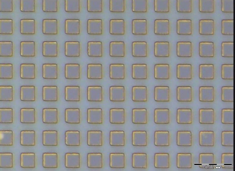
Figure 1.Optical microscope image of the mask pattern designed.
The profiles and morphologies of the InGaN/GaN microrings were investigated using SEM images. Optical properties of the samples were examined at room temperature using a SEM-based CL system at beam energy of 5 keV. The EL properties of the LED chips were characterized on a probe station for current injection and emission detection, and the light was collected by confocal microscopy.
3. RESULTS AND DISCUSSION
Figure 2 shows the top-view and cross-section SEM images of InGaN/GaN MQWs grown on the GaN microring structure. It is clear that the inner shape of the microrings is hexagonal, with a series of inclined facets in the inner side. Additionally, on the top surface, flat (0001) planes are observed between the microrings. The sidewall facets have an inclined angle of to the (0001) basal plane, as shown in Fig. 2(b). The identification is consistent with prior experiments in which pyramidal structures were grown under SAE with dot mask patterns [14]. Based on the standard projection, the inclined sidewall facets are identified as equivalent semi-polar {1-101} planes. It is suggested that the morphological changes of GaN microfacets under SAE are strongly related to the surface polarity and surface energy. Experimental results have proved that the {1-101} plane formation was more stable than that of other semi-polar planes under a wide range of growth conditions, and the morphology of a {1-101} plane was independent of growth parameters. Hence, the lateral and vertical growth rates were almost constant, leading to the smooth morphology composed of specific {1-101} facets with nitrogen polarity [15].

Figure 2.(a) Top-view and (b) cross-section SEM images of InGaN/GaN MQWs grown on a GaN microring structure.
Typical CL spectra from the {1-101} sidewall facets and (0001) flat surface of the InGaN/GaN MQWs are displayed in Fig. 3(a). Each spectrum has a peak near 365 nm that corresponds to the GaN underlying the microring QW. The InGaN/GaN MQWs on the {1-101} microfacet show an emission peak at about 445 nm, while the MQWs on the (0001) surface reveal an emission peak near 560 nm. A more detailed position dependence of CL emission has been examined from the inner {1-101} QW plane to the (0001) surface as the arrow direction indicated in the inset of Fig. 4, and Fig. 4 plots the CL peak wavelengths. As shown, the CL wavelength changes from 455 to 560 nm as the position moves from the inclined {1-101} QW plane toward the top (0001) surface, and the 365 nm emission wavelength corresponds to the GaN template under the MQWs.
Figure 3.(a) CL spectra from different facets of an InGaN/GaN MQW microring. Monochromatic CL intensity images over a single MQW microring at wavelengths of (b) 445 and (c) 560 nm.
Figure 4.Position dependence of the CL peak wavelength from the inner {1-100} plane to the top (0001) surface.
The result suggests a large redshift in emission wavelength for (0001) plane MQWs compared to inclined {1-101} plane MQWs, which is attributed to the indium content enrichment in the top (0001) plane MQWs. The indium enrichment originates from additional source supply due to the surface migration effect and lateral vapor-phase diffusion during the SAE process. The migration length of the group III atoms on the mask and their diffusion lengths in the vapor phase are ordered according to [16]. Therefore, indium enrichment during SAE occurs due to the enhanced supply of In species from the inclined facets to the top surface. Hence, InGaN/GaN MQWs with a longer emission wavelength on the top (0001) surface have been achieved.
Figure 5 shows the photo image of the fabricated LED chip with diameter of 350 μm. Typical white-light EL at 50 mA was achieved on-wafer under DC conditions, confirming the excellent performance of our white LEDs. Figure 5 shows the EL spectra of the microring white LEDs, measured for DC drive currents ranging from 30 to 200 mA. The current–voltage (I–V) characteristics of the white LEDs have been plotted in the inset of Fig. 5. The forward voltage at 20 mA is about 5.5 V, and the value is higher than those of conventional InGaN/GaN MQW LEDs. This can be attributed to the reduced effective contact to the p-type GaN layer of the devices, because some p-contact metals are directly deposited on masks [17].
Figure 5.Photo image of EL at a 50 mA forward drive current for the fabricated LED chip wafer. The inset shows the surface pattern image of a single LED chip.
The EL spectra were measured to investigate the optical properties of the LED. Figure 6 shows the EL spectra of the LED with increasing injection current; two EL emission peaks at about 445 and 560 nm were mixed, showing near white emission (shown in Fig. 4). The long wavelength of 560 nm emission is from MQWs grown on the c-plane (0001), which is on top of the microrings, because the c-plane (0001) provides higher In composition in InGaN QWs than semi-polar {1-101} microfacets. On the other hand, the blue emission peak around 445 nm is from MQWs grown on semi-polar {1-101} microfacets. The results are well consistent with the CL spectra. It also can be observed that both EL emission peaks show blueshifts at high injection currents due to Coulomb screening of the quantum confined Stark effect induced by the piezoelectric polarization and the band-filling effect. The EL emission from semi-polar {1-101} MQWs shows a small blueshift of about 3 nm, while the EL emission from MQWs on the c-plane (0001) shows a large blueshift of 15 nm with increasing injection current from 30 to 200 mA. These results are attributed to large polarization-induced electric fields in the MQWs grown on c-plane (0001) GaN compared with those grown on semi-polar GaN.
Figure 6.EL spectra of white LED with increasing injection current. The inset shows the I–V characteristics of the LED.
4. CONCLUSIONS
In conclusion, we demonstrate white EL emission of LEDs with InGaN/GaN MQWs grown on GaN microrings, which are composed of semi-polar {1-101} microfacets and a c-plane (0001). The CL and EL spectra confirm that the white-light emission originates from the mixture of blue wavelength of about 445 nm and long wavelength of 560 nm emitted from the InGaN/GaN MQWs on semi-polar and (0001) facets. The variation of emission wavelength on different facets is attributed to the lateral vapor diffusion and surface migration of III group atoms during SAE growth. These results suggest the possibility to realize white LEDs using the geometry of GaN microfacets without phosphors, which is a promising advancement for future optoelectronic device designs.
Acknowledgment
Acknowledgment. This work was financially supported by the Natural Science Foundation of Jiangsu Province (Nos. BK20150158, BK2011436, and BM2014402), the China Postdoctoral Science Foundation (Nos. 2014M561623 and 2014M551559), Jiangsu Planned Projects for Postdoctoral Research Funds (No. 1401013B), and the Fundamental Research Funds for Central Universities (Nos. JUSRP51517 and JUSRP11408).
References
[1] G. Heliotis, P. N. Stavrinou, D. D. C. Bradley, E. Gu, C. Griffin, C. W. Jeon, M. D. Dawson. Spectral conversion of InGaN ultraviolet microarray light-emitting diodes using fluorine-based red-, green-, blue-, and white-light-emitting polymer overlayer films. Appl. Phys. Lett., 87, 103505(2005).
[2] E. F. Schubert, J. K. Kim. Solid-state light sources getting smart. Science, 308, 1274-1278(2005).
[3] C. F. Huang, C. F. Lu, T. Y. Tang, J. J. Huang, C. C. Yang. Phosphor-free white-light light-emitting diodes of weakly carrier-density-dependent spectrum with prestrained growth of InGaN/GaN quantum wells. Appl. Phys. Lett., 90, 151122(2007).
[4] Y. L. Li, T. Gessmann, E. F. Schubert, J. K. Sheu. Carrier dynamics in nitride-based light-emitting p-n junction diodes with two active regions emitting at different wavelengths. J. Appl. Phys., 94, 2167-2172(2003).
[5] S. C. Shei, J. K. Sheu, C. M. Tsai, W. C. Lai, M. L. Lee, C. H. Kuo. Emission mechanism of mixed-color InGaN/GaN multi-quantum-well light-emitting diodes. Jpn. J. Appl. Phys., 45, 2463-2466(2006).
[6] J. W. Shi, H. Y. Huang, C. K. Wang, J. K. Sheu, W. C. Lai, Y. S. Wu, C. H. Chen, J. T. Chu, H. C. Kuo, W. P. Lin, T. H. Yang, J. I. Chyi. Phosphor-free GaN-based transverse junction light emitting diodes for the generation of white light. IEEE Photon. Technol. Lett., 18, 2593-2595(2006).
[7] I. K. Park, J. Y. Kim, M. K. Kwon, C. Y. Cho, J. H. Lim, S. J. Park. Phosphor-free white light-emitting diode with laterally distributed multiple quantum wells. Appl. Phys. Lett., 92, 091110(2008).
[8] Y. J. Lee, P. C. Lin, T. C. Lu, H. C. Kuo, S. C. Wang. Dichromatic InGaN-based white light emitting diodes by using laser lift-off and wafer-bonding schemes. Appl. Phys. Lett., 90, 161115(2007).
[9] S. Srinivasan, M. Stevens, F. A. Ponce, T. Mukai. Polychromatic light emission from single InGaN quantum wells grown on pyramidal GaN facets. Appl. Phys. Lett., 87, 131911(2005).
[10] K. Nishizuka, M. Funato, Y. Kawaami, Y. Narukawa, T. Mukai. Efficient rainbow color luminescence from InxGa1-xN single quantum wells fabricated on {11-22} microfacets. Appl. Phys. Lett., 87, 231901(2005).
[11] M. Funato, K. Hayashi, M. Ueda, Y. Kawakami, Y. Narukawa, T. Mukai. Monolithic polychromatic light-emitting diodes based on InGaN microfacet quantum wells toward tailor-made solid-state lighting. Appl. Phys. Express, 1, 011106(2008).
[12] M. Feneberg, K. Thonke. Polarization fields of III-nitrides grown in different crystal orientations. J. Phys., 19, 403201(2007).
[13] G. F. Yang, P. Chen, M. Y. Wang, Z. G. Yu, B. Liu, Z. L. Xie, X. Q. Xiu, Z. L. Wu, F. Xu, Z. Xu, X. M. Hua, P. Han, Y. Shi, R. Zhang, Y. D. Zheng. Selective epitaxy of InGaN/GaN multiple quantum wells on GaN side facets. Phys. E, 45, 61-65(2012).
[14] K. Hiramatsu, K. Nishiyama, M. Onishi, H. Mizutani, M. Narukawa, A. Motogaito, H. Miyake. Fabrication and characterization of low defect density GaN using facet-controlled epitaxial lateral overgrowth (FACELO). J. Cryst. Growth, 221, 316-326(2000).
[15] H. Marchand, J. P. Ibbetson, P. T. Fini, S. Keller, S. P. DenBaars, J. S. Speck, U. K. Mishra. Mechanisms of lateral epitaxial overgrowth of gallium nitride by metalorganic chemical vapor deposition. J. Cryst. Growth, 195, 328-332(1998).
[16] T. Tsuchiya, J. Shimizu, M. Shirai, M. Aoki. InGaAlAs selective-area growth on an InP substrate by metalorganic vapor-phase epitaxy. J. Cryst. Growth, 276, 439-445(2005).
[17] H. W. Choi, M. D. Dawson, P. R. Edwards, R. W. Martin. High extraction efficiency InGaN micro-ring light-emitting diodes. Appl. Phys. Lett., 83, 4483-4485(2003).

