
Leena Singh, Weili Zhang, "Advancements in high refractive index media: from quantum coherence in atomic systems to deep sub-wavelength coupling in metamaterials [Invited]," Chin. Opt. Lett. 18, 062401 (2020)
- Chinese Optics Letters
- Vol. 18, Issue 6, 062401 (2020)
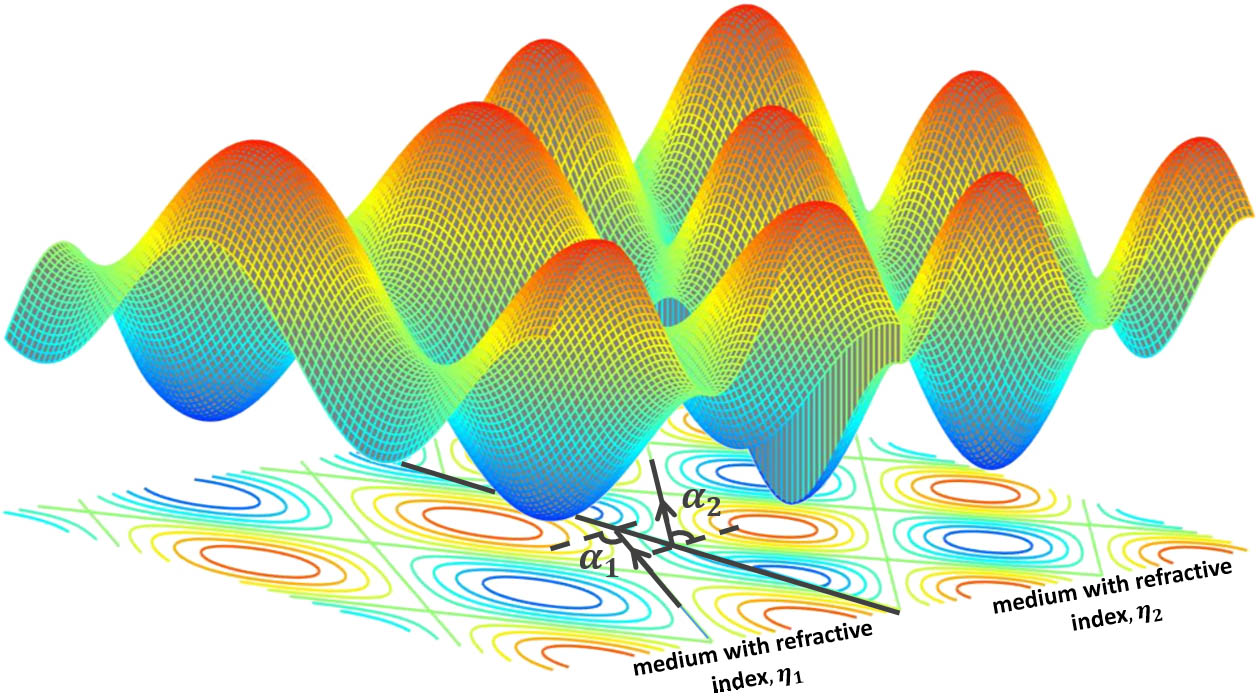
Fig. 1. Bending of an electromagnetic wave while passing from one medium to another with different refractive indices. An electromagnetic wave traveling at an angle of
![Dispersive (Re P) and absorptive (Im P) parts of polarization versus detuning of radiation frequency from midpoint between levels b′ and b. The polarization is plotted on an arbitrary scale, and detuning Δ is plotted in units of atomic decay. Inset, upper right-hand corner: usual dispersion-absorption curve. Inset, upper left-hand corner: present level scheme. Reprinted with permission from Ref. [5], copyright by the American Physical Society.](/richHtml/col/2020/18/6/062401/img_002.jpg)
Fig. 2. Dispersive (Re P) and absorptive (Im P) parts of polarization versus detuning of radiation frequency from midpoint between levels
Fig. 3. Schematic of the metal film with periodic slits. The parameters are defined as in the figure:
Fig. 4. Metal surface with periodic holes drilled (above) and equivalent waveguide structure (below). Reprinted with permission from Ref. [36], copyright by the AIP Publishing.
Fig. 5. (a) Unit cell of metal cubes that were arranged in a cubic array fashion; all the six surfaces of these cubes consisted of air slits and were interconnected by three orthogonal wires along with the simplified structure (left) with two plates with air slits and a connecting wire along the z direction. Reprinted with permission from Ref. [40], copyright by the American Physical Society. (b) A layered view of bulk materials formed with a unit cell of single cut wire on a dielectric substrate. (c) An I-shaped metallic patch structure. (d) A terahertz metamaterial with Z-shaped meta-atoms.
Fig. 6. Ultrathin terahertz metamaterial with a double-sided metal structure depicting a deep subwavelength coupling absence (above) and presence (below) between the metal structures situated on both sides of an ultrathin dielectric substrate. Reprinted with permission from Ref. [50], copyright by the AIP Publishing.


Set citation alerts for the article
Please enter your email address

© Copyright 2018-2021 | Chinese Laser Press. All Rights Reserved 沪ICP备15018463号-20