Leena Singh, Weili Zhang, "Advancements in high refractive index media: from quantum coherence in atomic systems to deep sub-wavelength coupling in metamaterials [Invited]," Chin. Opt. Lett. 18, 062401 (2020)
Copy Citation Text
Refractive index enhancement is crucial in the fields of lithography, imaging, optical communications, solar devices, and many more. We present a review of advancements in the process of designing high refractive index metamaterials, starting from quantum coupling and photonic bandgap materials to metamaterials utilizing deep subwavelength coupling to achieve ever-high values of refractive index. A particular attention is given to experimentally verified schemes in engineering a high index of refraction. The understanding of the evolution of material design from intrinsic electronic states manipulation to meta-atoms design is not only fascinating but also a prerequisite to developing successful devices and applications.
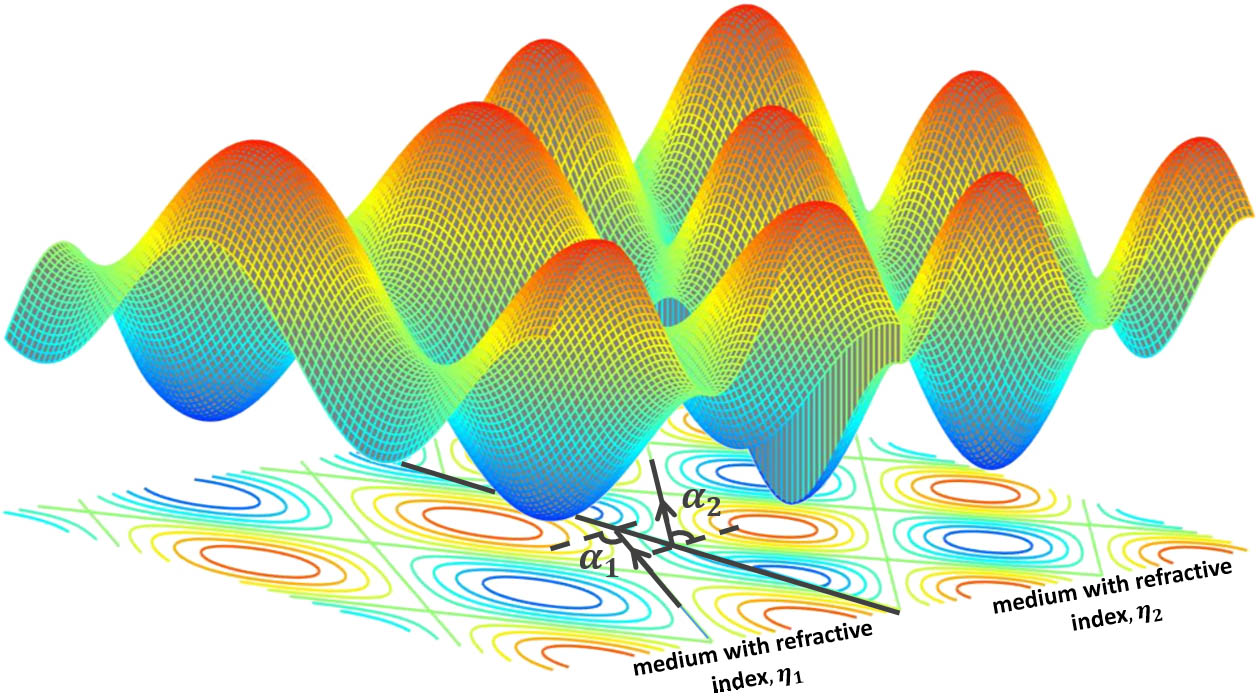
Materials with a modified refractive index have long been a part of human history. An impressive application of a modified refractive index can be found in the form of the well-known stained glass art windows at the 13th century Notre Dame cathedral in Paris. Refractive index is basically defined as a dimensionless quantity that measures the bending of the electromagnetic wave while passing from one medium to another, as shown in Fig. 1.
Figure 1.Bending of an electromagnetic wave while passing from one medium to another with different refractive indices. An electromagnetic wave traveling at an angle of with respect to the normal in a medium with a refractive index undergoes refraction at the medium interface and travels at an angle of with respect to the normal in a medium with a refractive index .
In 1621, Dutch astronomer and mathematician Willebrord Snell defined the relation between the ratio of the refractive indices of the two media and the ratio between the angle of incidence and angle of refraction as
By the 19th century, a number of scientific journals had already been discussing the potential applications of high refractive index media for laser particle acceleration[1,2], optical microscopy[3], atomic tests of electroweak physics[4], and magnetometry[5]. In 1991, Scully presented the possibility of achieving, in principle for the first time[5], a high refractive index in a three-level atom in the lambda configuration without high absorption via quantum coherence. Index enhancement was accomplished by choosing to operate near an atomic resonance between a coherent ground-state doublet configuration and and an excited state with level probabilities , along with an appropriately chosen atom-field detuning[5]. The result is shown in Fig. 2, with a large dispersion marked as point B and a near zero absorption marked as point C.
Sign up for Chinese Optics Letters TOC. Get the latest issue of Chinese Optics Letters delivered right to you!Sign up now
Figure 2.Dispersive (Re P) and absorptive (Im P) parts of polarization versus detuning of radiation frequency from midpoint between levels and . The polarization is plotted on an arbitrary scale, and detuning is plotted in units of atomic decay. Inset, upper right-hand corner: usual dispersion-absorption curve. Inset, upper left-hand corner: present level scheme. Reprinted with permission from Ref. [5], copyright by the American Physical Society.
Coherence between levels and can be achieved by a number of techniques, i.e., the pulse[6], microwave[7], or Raman technique[8,9]. In 1992, Fleischhauer et al. presented a detailed survey of various schemes in which atomic coherence and interference effects lead to complete absorption cancellation and an ultrahigh index of refraction[10].
In 1994, Dowling et al. proposed photonic bandgap materials as a possible candidate to achieve a high index of refraction and presented a quantitative study explaining the anomalous index of refraction in photonic bandgap materials[11]. The term photonic bandgap was introduced for the first time in 1979 by Ohtaka[12] when he established the theory of low energy photon diffraction (LEPD) in analogy with the theory of low energy electron diffraction (LEED). However, it was in 1990 when the first experimental three-dimensional (3D) photonic bandgap made in a periodic dielectric structure was demonstrated by Ho et al.[13]. Dowling’s study was based on the one-dimensional (1D) periodic dielectric array that was used to model a 3D photonic bandgap material to enhance the effective refractive index. He explained that near the gap in the photonic bandgap materials the effective index of refraction can become less than unity and, in fact, can approach zero at the band edge itself leading to the ultra-refractive optical effect[11]. Given that the refractive index of a system is the ratio , his scheme was based on a decreasing instead of an increasing , to obtain a high effective refractive index[11]. In 1996, Zibrov et al. presented a proof-of-principle experiment demonstrating a resonantly enhanced refractive index and a reduced absorption achieved by quantum coherence in Rb vapor[14]. A resonant change of about in the refractive index was observed.
Recently after that, in 1998 Uzma et al. proposed a two-level atom damped by an off-resonance squeezed vacuum field for refractive index enhancement with a vanishing absorption. With the application of a squeezed vacuum field, index enhancement effect can be obtained without any coherent laser fields coupled to the system[15]. By the end of 1999, advancements in microfabrication techniques added ease to the fabrication of artificial media. In addition to 3D structures, two-dimensional (2D) thin film, and structures with metallic components within the unit cells, metallo-dielectric structures have also begun to attract scientific attention, as the physics associated with the metallo-dielectric structures was quite unique and very different from the pure dielectric structures[16]. In 2000, two very intriguing candidates for refractive index enhancement emerged: the first was a non-resonant heterogeneous medium composed of small metallic clusters (nanoballs) suspended in transparent matrix studied by Oraevskii et al.[17] and the second was associated with intersubband transition in an n-type asymmetric double quantum well semiconductor system studied by Sadeghi et al.[18]. Both the two schemes later formed a strong basis for more intensive research areas[19–24].
In 2001, the term metamaterial was first defined by Welser as “macroscopic composites having a man-made, 3D, periodic cellular architecture designed to produce an optimized combination not available in nature, of two or more responses to a specific excitation. Each cell contains metaparticles, macroscopic constituents designed with low dimensionality that allows each component of the excitation to be isolated and separately maximized. The metamaterial architecture is selected to strategically recombine local quasi-static responses, or to combine or isolate specific non-local responses”[25]. In 2002, Zibrov et al. performed another experimental study for resonant enhancement of the refractive index in a cascade scheme and observed that some coherence is preserved in a thin boundary layer, even in atomic gas with a vapor density of , which leads to a resonant enhancement of the refractive index[26]. However, the problem of attaining a high refractive index and small absorption in a highly dense atomic medium remained unsolved. Meanwhile, the resonant enhancement of the refractive index was still being intensively explored in different atomic[27] and solid state systems[28,29]. In 2005, Yavuz proposed a scheme to achieve a refractive index enhancement with a vanishing absorption, even in a far-off resonant atomic system. It was achieved by exciting two Raman resonances with approximately chosen strong control lasers[30].
In 2005, Shen et al. explained the mechanism for designing a high refractive index metallic metamaterial. Shen et al. claimed that a metallic film with periodic 1D cut-through slits can be considered as a dielectric slab with an effective refractive index and a width , as shown in Fig. 3[31].
Figure 3.Schematic of the metal film with periodic slits. The parameters are defined as in the figure: is the width of the slit, d is the periodicity, and L is the thickness of the metal film. The black regions indicate the metal parts, and the white regions are the vacuum. The film is extended in the plane. Reprinted with permission from Ref. [31], copyright by the American Physical Society.
The effective “n” is determined by a field comparison between the metallic film with a periodic cut through the slits and the dielectric slab. Given the periodicity of the slits in the metallic film is smaller than the wavelength, the zeroth-order transmission amplitude of a TM wave normally incident on the metallic film can be written as[31]where is the filling factor of the slit and , for normal incidence; and . When a plane is normally incident on a dielectric slab with a refractive index , the transmission amplitude can be written as
Comparing Eqs. (2) and (3), both transmission amplitudes and can be approximately equalized by setting and [31]. With the transmission equivalence set up and establishing the effective refractive index as , which is defined only by the geometry of the structure, Shen et al. pointed out that the refractive index of a medium can be enhanced without having to change the intrinsic electronic states of the material. The paradigm of high refractive index medium design is now shifting toward controlling the behavior of the electromagnetic waves by virtue of the structural geometry of the artificial media to achieve desired material parameters, namely, permeability and permittivity, rather than meddling with the atomic states of the media.
This range of frequencies from 1 to 3 THz is extremely fascinating as it witnesses the breakpoint of both electrical and magnetic responses in most of the naturally occurring materials. The terahertz regime is the slice of the spectrum that lies between the infrared and microwave radiations. In spite of the fact that terahertz technology has had very diverse and attractive applications in the fields of astronomy, semiconductor, medical imaging, atmospheric studies, space communication, defense, and so on, it remains the least-developed region due to the lack of materials responding to or at these frequencies[32,33]. The advent of metamaterials has proven to be especially valuable in the terahertz regime and expected to close the “THz gap”. Following the same structure of metallic film with periodically arranged cut-through slits, theoretically conversed by Shen et al., Pimenov and Loidl performed the first experimental demonstration for a high refractive index metamaterial at terahertz frequencies in 2006. A terahertz high refractive index metamaterial was fabricated using high purity copper plates with periodic slits[34]; a Mach–Zehnder interferometer arrangement[35] was then used to carry out the experiment for the frequency range of 60 to 380 GHz; and the reflectance and the complex transmittance were measured. The effective parameters of the sample were obtained with Fresnel optical formulas for reflectance and transmittance using the equations
Here, and , is the reflection amplitude at the air-sample interface, is the “pure” transmission amplitude, is the complex refractive index, is the sample thickness, and is the radiation wavelength[34]. An effective refractive index 5.51 was obtained and an additional correction was suggested to be added to the experimentally obtained phase in order to establish the equivalence to the real dielectric slab. This metal-dielectric interface can support surface plasmon waves in the optical regime.
The dispersion curve of these surface plasmon waves is relatively flat at high frequencies and can be used to slow down light. In the low frequency (microwave) regime, however, metal is treated as a perfect electric conductor (PEC), which means electromagnetic waves cannot penetrate into metal and hence metal-dielectric interfaces cannot support surface waves. So, instead of cut-through slits or a metal-dielectric interface, an array of holes drilled in metal surface was used to achieve slow electromagnetic waves[36–38]. The schematic and numerical comparison between the metal dielectric structure and metallic hole structure are elaborated in Fig. 4[36].
Another proof of principle experiment was performed in 2008 by Proite et al.[39] validating Yavuz’s scheme[30] to achieve a refractive index enhancement with a vanishing absorption using two Raman resonances in far-off resonant atomic systems. The experiment was performed by driving alkali atoms in a vapor with appropriate control lasers, and inducing one gain resonance and other absorption resonances for a probe beam in a two-photon Raman configuration[39]. A maximum refractive index of 2 was observed for an alkali vapor at a density of .
Figure 4.Metal surface with periodic holes drilled (above) and equivalent waveguide structure (below). Reprinted with permission from Ref. [36], copyright by the AIP Publishing.
In 2009, two intriguing structural schemes were simulated to achieve a high index of refraction. One was a broad bandwidth 3D structure proposed by Shin et al.[40] while the other was a resonance-based structure by Shi et al.[41]. Shin’s structure consisted of metal cubes that were arranged in a cubic array fashion, and all six surfaces of these cubes consisted of air slits and were interconnected by three orthogonal wires, as shown in Fig. 5(a). The structure was based on the observation that the induced charges due to a normal electric field determine the effective relative permittivity while the induced surface current due to a parallel magnetic field contributes to the effective relative permeability [40]. For a large cube limit (i.e., ), permittivity and permeability can be estimated using the equations where is the side of the cube and represents the periodicity[40]. The simulated structure was able to enhance the refractive index over a broad bandwidth by maintaining a permeability near unity via reducing the area subtended by the current loops owing to the air slits in the surface and thereby suppressing the diamagnetic response. Meanwhile, the permittivity of the structure is enhanced by upholding a strong capacitive response within the cubic array. The other salient scheme, which was proposed by Shi et al., was based on electric resonance in the surface structures to enhance the effective refractive index[41].
Figure 5.(a) Unit cell of metal cubes that were arranged in a cubic array fashion; all the six surfaces of these cubes consisted of air slits and were interconnected by three orthogonal wires along with the simplified structure (left) with two plates with air slits and a connecting wire along the z direction. Reprinted with permission from Ref. [40], copyright by the American Physical Society. (b) A layered view of bulk materials formed with a unit cell of single cut wire on a dielectric substrate. (c) An I-shaped metallic patch structure. (d) A terahertz metamaterial with Z-shaped meta-atoms.
Shi’s configuration, shown in Fig. 5(b), is a planar structure of a periodic arrangement of metallic wires on a dielectric substrate of subwavelength thickness, which was then layered to achieve a bulk metamaterial. The value of the maximum effective refractive index of the metamaterial was characterized using the Bloch wave method and was defined using the equation where is the resonance angular frequency, is the propagation constant at the resonance, is the wave number at the resonance frequency, and is the periodicity of the structure[41]. The length of the metallic subwavelength wires controlled the resonance frequency while the propagation constant corresponding to a higher refractive index around the resonance is governed by the number of layers along the direction of propagation of the electromagnetic wave. This resonance-based scheme offered a contrast to the previous prevalent methods, which achieved a high refractive index by the confinement of electromagnetic mode in the subwavelength region, i.e., the propagation TEM mode in the slits and the evanescent mode in the holes below the cutoff[41]. This metallic wire array metamaterial design was soon after experimentally verified and analyzed by Wei et al. in 2010, to achieve a high refractive index value at visible frequencies with a metamaterial fabricated using quartz as a dielectric substrate and silver to form a cut wire structure[42].
In 2011, Choi et al. exquisitely combined both Shin’s[40] and Shi’s[41] schemes to demonstrate a high refractive index value at terahertz frequencies. The resonating subwavelength cut wire structure in Shi’s scheme was replaced with an ‘I’-shaped metallic patch[43], an abridged 2D version of Shin’s slited cube structure. The resultant metamaterial structure, shown in Fig. 5(c), is capable of producing a high effective permittivity due to the capacitive behavior while maintaining a low diamagnetic response due to the smaller current-loop area. Choi’s metamaterial was fabricated on flexible, thin film polyimide substrate. The metallic structure was created using gold (on chromium). A periodic array of thus created unit cells was then layered on top of each other, similar to Shi’s scheme, to investigate the bulk properties of the metamaterial. The band structure and the dispersion relation of the fabricated metamaterial were investigated to understand the effect of the number of layers on the electromagnetic characteristics of the bulk media. The maximized transmission of the slab is defined by the equation where is the transmission peak frequency, is a non-negative integer, is the number of layers, is the speed of light, and is the thickness of each layer[43]. Choi et al. experimentally achieved a refractive index as high as 38.64 at 0.315 THz and claimed that higher values of refractive index can be achieved by reducing the distance between the individual I-shaped metallic patches or the spacing between layers until the gap width reaches the Thomas–Fermi length scale[44] or the quantum tunneling scale of electrons. In 2012, Simmons et al. furthered Proite et al.’s experiment[39] to short alkali-vapor cells with densities exceeding and demonstrated a refractive index change of about [45].
The exact 3D structure of metallic cubes arranged in a cubic array fashion proposed by Shin et al.[40] was experimentally demonstrated in the microwave regime by Campbell et al. in 2013[46]. Campbell et al. fabricated two samples, one with an array of solid copper cubes and the other with an array of structured copper cubes. Both of the samples were characterized using the strip line method for material characterization pioneered by Barry in 1986[47]. The comparison of the experimentally obtained material parameters of the solid cubes with that of the structured cubes revealed that the real part of the permittivity of the structured cube sample was approximately half that of the solid cube sample, but the refractive index was still nearly doubled since the structured cubes facilitated a reduced diamagnetic response resulting in an almost six-fold increase in the effective permeability value[46]. Tan et al. furthered Choi’s I-shaped metallic patch structure[43] with a Z-shaped meta-atom in 2015[48], as shown in Fig. 5(d). The Z-shaped meta-atom was capable of attaining a high refractive index at a lower frequency by virtue of the existence of a parallel, unidirectional surface current in the two arms of the structure that leads to a larger effective induction compared to that in the I-structure and thus lowers the resonance frequency without having to reduce the size of the overall structure. The Z-structure metamaterial was fabricated via the conventional lithography using an aluminum and thin film polyimide substrate. Time-domain terahertz spectroscopy characterization revealed a 21.6% average shift in the resonance frequency[48]. This simple design modification offered a great ease in the fabrication of high refractive index metamaterials operating at lower frequencies. In 2016, Chang et al. reported a broadband refractive index scheme based on mesoscopic space-filling curves. He claimed a gigantic dielectric constant enhancement due to displacement between the layers resulting in a very high displacement enhancement factor[49].
Although these approaches were able to enhance the refractive index to unnatural values, the highest values of refractive indices achievable with these schemes are demarcated mainly due to two reasons. First, the limit posed by the number of layers that can be productively used at a particular frequency, dictated by Eq. (8). Second, the practical limit to which the periodicity of the meta-atoms can be decreased before losing the capacitance effect all together.
In 2017, we proposed a terahertz metamaterial design capable of achieving ever higher values of refractive index owing to a very high effective permittivity realized by employing a deep subwavelength coupling between the arrays of identical structures situated on both sides of an ultrathin dielectric film, as shown in Fig. 6[50].
Figure 6.Ultrathin terahertz metamaterial with a double-sided metal structure depicting a deep subwavelength coupling absence (above) and presence (below) between the metal structures situated on both sides of an ultrathin dielectric substrate. Reprinted with permission from Ref. [50], copyright by the AIP Publishing.
Owing to the subwavelength thickness of the substrate film, the metal structures situated on both of its sides got coupled generating tremendous capacitive response in addition to the capacitance due to the nearest neighbor coupling between structures on the same side. Meanwhile, the permeability of the metamaterial remained near unity due to the small current loop area subtended by the checkboard metal structure. An array of isotropic checkboard structure was fabricated by thermal deposition of aluminum on both sides of the polyimide substrate film with thickness 22 and μ, respectively. Using terahertz time domain spectroscopy, both the samples were characterized and the calculated effective refractive index for the μ thick sample was found to be increased to 41.8 as compared to the 7.78 refractive index for the μ thick sample and can be further increased to 77.02 for a 100 nm thick sample. The enhancement of the refractive index can be further boosted by increasing deep subwavelength coupling between meta-atoms on the opposite side of the spacer layer either by decreasing the substrate layer thickness or selecting a substrate of a higher refractive index or both. The effective refractive index of the metamaterial governed dominantly by the inter-layer deep subwavelength coupling demonstrated a universal power law behavior [described by Eq. (10)] with respect to the substrate thickness, and a linear behavior [described by Eq. (11)] with respect to the substrate refractive index, where , , , and are the constants that depend on the metamaterial structure, is the substrate film thickness, and is the substrate refractive index. Although it was predicted by many previous schemes[31,41,43] that decreasing the thickness of individual designer layers of the bulk metamaterial would enhance the refractive index values, it was the first time that reducing the substrate thickness to subwavelength levels was utilized to facilitate coupling effect between the resonating structures fabricated on both the sides of the substrate layer. This enabled the attainment of tremendous effective permittivity and thus an ultra-high value of the effective refractive index of the metamaterial.
The quest for designing a high refractive index medium, initiated in an atomic system with the help of quantum coherence, reached up to a highly matured science of periodically designed structures known as metasurfaces/metamaterials. The terminology and understanding of the system design limited to quantum coherence in the initial atomic systems also mellowed with powerful structures capable of utilizing deep subwavelength coupling. Pendry et al. stated that “it is only one small step to replace the atoms of the original concept with structures on a large scale” as every material can be considered composite even if the individual constituents are atoms or molecules[51]. Moreover, the atomic and molecular systems are quite restrictive when it comes to designing higher values of permeability, particularly for frequencies at the gigahertz range where the magnetic response of most materials begins to fade away[51]. At these frequencies, microstructuring is a very helpful technique with a simple restriction on the unit cell size of where is the unit cell size and is the radiation frequency[51]. Once the above condition is met, longer wavelengths are unable to resolve the internal structure and hence perceive the microstructured medium as homogenous or, in other words, the same as the atomic systems for the shorter wavelengths. Thus, microstructures provided a great ease and flexibility in terms of choosing materials and structural design and have a far more capability of manipulating electromagnetic responses compared to the atomic counterpart.
It is crucial to mention that although it is okay to achieve higher values of refractive index solely by enhancing the effective permittivity of the medium, the fact that permeability is also an integral part of the refractive index equation cannot be ignored. There have been a number of reports[52,53] on high refractive index metamaterial with miscalculated or unexplained permeability values above unity. The metamaterial structures discussed in these reports may be capable of refractive index enhancement, as evident from the logical arguments presented in these reports, but just not as high as that reported, the miscalculated values are misleading and hence need to be revisited for due corrections. Resonance-based schemes[52,53] miscalculated the permeability to be higher than unity even in the absence of resonance. This is due to the fact that the measured transmission is not properly compensated to account for the experimental setup while plugging the measured values for calculating refractive index. Once calculations are set right, the resulting permeability values would be reduced, which would lead to a discrepancy in the reported refractive index values.
In conclusion, the science of designing a high refractive index medium has come a long way since meddling with the intrinsic state of matter to the design of metamaterials with perpetually imaginative structures. It may not be even far-fetched to assume that the high refractive index medium design with static values of refractive indices have been quite saturated. In recent years the research focus has shifted more toward devising media capable of dynamic enhancement of the refractive index[54,55] by means of electrical stimuli. The incredible scientific endeavors leading to the realization of thin film, broadband, dynamic control, and ultra-high refractive index media are sure to play a crucial role in shaping the face of modern-day devices.
Leena Singh, Weili Zhang, "Advancements in high refractive index media: from quantum coherence in atomic systems to deep sub-wavelength coupling in metamaterials [Invited]," Chin. Opt. Lett. 18, 062401 (2020)