Abstract
In this Letter, new concepts of fluorescence phase-change materials and fluorescence phase-change multilevel recording are proposed. High-contrast fluorescence between the amorphous and crystalline states is achieved in nickel- or bismuth-doped phase-change memory thin films. Opposite phase-selective fluorescence effects are observed when different doping ions are used. The fluorescence intensity is sensitive to the crystallization degree of the films. This characteristic can be applied in reconfigurable multi-state memory and other logic devices. It also has likely applications in display and data visualization.Memory effects and data storage devices based on the transition between the amorphous and crystalline phases or states in chalcogenide alloys, such as GeSbTe, have attracted scientific and industrial interest over the past 40 years[1–3]. In addition, the development of binary phase-change memories, including rewritable optical disks and random access memory, predominates, multi-state (multi-level or multi-bit) memories will attract considerable interest in the future, because these memories offer a high storage density.
Injecting new states into phase-change materials is one of the most important issues in this field. Multi-state phase-change memory thin films were first reported by Ovshinsky in his early work and continued refinements[4,5]. Optical or electrical programming modulates the crystallization degree of a film; consequently, the intermediate reflectance or resistance states of these films can be easily obtained[6]. About four to six orders of magnitude is the maximum difference in electrical resistivity between the amorphous and crystalline states. This maximum difference can result in more states and higher contrasts between films. The optical reflectivity contrast between the amorphous and crystalline states is commonly . The detection of the reflective intensity greatly limits the number of multiple states in applications. Effective ways to obtain the difference in optical signals with high contrast in multi-state phase-change optical memories should be developed.
Fluorescence detection as an information readout method is capable of attaining a higher contrast or signal-to-noise ratio than the traditional reflectance detection readout method. However, fluorescence readout has only been applied in photon-mode recording media, especially in some organic materials, such as photochromic[7] or two-photon absorption molecules[8]. The currently known fluorescent memory materials are not prepared using phase-change materials. Phase-change memory materials that are typically used in the thermal mode are non-luminescent.
Sign up for Chinese Optics Letters TOC. Get the latest issue of Chinese Optics Letters delivered right to you!Sign up now
This Letter reports the phase-selective fluorescence effects of doped (GST) phase-change memory thin films. The luminescence property of a film can be switched on and off by controlling the phase transition in these films. Opposite fluorescent properties can be realized by doping thin films with different luminescent ions. Multi-state fluorescence can be achieved by modulating the crystallization degree of films. A fluorescence phase-change memory material prepared using this method retains the different optical and electrical properties of the amorphous and crystalline states. These properties can be applied in reconfigurable memory and logic devices. It also has likely applications in display and data visualization. The luminescence effects of phase-change materials will more powerfully enhance the optical contrast and color switching performances when compared with refractive index transformation[9] and thickness adjustment[10].
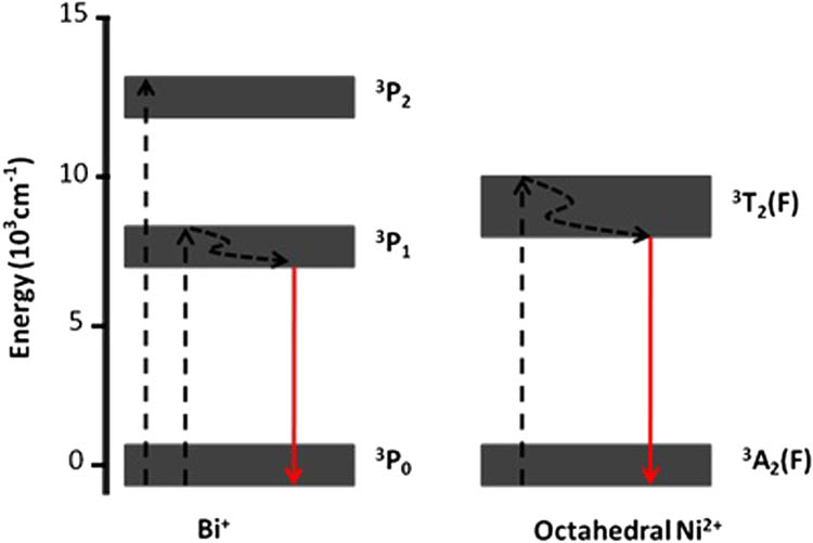
Designing phase-change materials is the first step in this process. These phase-change materials should be capable of emitting light. Most phase-change memory materials are prepared using an as-deposited chalcogenide glass. The luminescent doping ions in glass can be used in phase-change materials. Nickel () and bismuth () ions are commonly used as active centers in broadband luminescence obtained in the near-infrared (NIR) wavelength range. They exhibit different luminescence conditions in different kinds of matrices (e.g., glass or crystal) because electronic transitions in their outermost or orbitals are strongly influenced by their ligands environments[11]. The luminescence of ions is often observed in crystals, such as , MgO, , , , , , and [12–19]. Only ions in an octahedral coordination state contribute to the emission of light. In this case, the luminescence is too weak to be observed in a glass matrix. This weak luminescence is caused by the high non-radiative transition probability and low quantum efficiency of ions. Conversely, the luminescence of Bi is often observed in glasses, such as silicate, germanate, borate, and phosphate, among others[20–23]; however, emissions of Bi in a crystalline matrix are seldom reported[24,25]. The emission center of Bi-doped glass is still highly debated, but more evidence indicates that it may be or even a lower valence state of Bi, such as clusters. Although the mechanism of luminescence is not clear, modifiers including , , , and with stable tetrahedron or unstable octahedral structures in a glass network remarkably affect the luminescence of ions. Figure 1 shows the energy level diagram for the luminescence of the in crystals and ions in silicate glasses. These ions were chosen as doping ions in a phase-changeable chalcogenide matrix.
![Energy level transition diagram of luminescence of Ni2+ in ZnAl2O4 crystals and Bi+ in silicate glasses as shown in Ref. [11].](/Images/icon/loading.gif)
Figure 1.Energy level transition diagram of luminescence of in crystals and in silicate glasses as shown in Ref. [11].
GST was chosen as the matrix in the luminescence ion doping. The similarity of the coordination fields in some oxide crystals/glasses and chalcogenides in the crystalline/amorphous states may provide similar conditions for luminescence. Te atoms in the rock salt-like crystal phase of GST occupy one sub-lattice of the crystal, and Ge and Sb atoms and vacancies randomly occupy the second sublattice of the crystal[26,27]. A Ge atom within a Te face-centered cubic lattice switches between octahedral and tetrahedral symmetry sites when GST undergoes a phase transition[28–31]. If the doping ions occupy suitable sites, such as the sites of the Ge, Sb, or vacancies, then the luminous conditions are satisfied, and the reversible phase-change feature with different doping ions can be maintained.
The Ni- or Bi-doped GST thin films were prepared by co-sputtering the NiO or Bi with the GST targets. The films were prepared in an Ar atmosphere with a pressure of 0.85 Pa and an Ar flow rate of 80 sccm. The required base pressure in the vacuum chambers was . The doping concentration of the or the ion was controlled by changing the sputtering power. The doping concentration was determined using an energy-dispersive spectrometer equipped with a scanning electron microscope (JEOL JSM-6360LA). The as-deposited thin films were crystallized by thermal annealing or initialization with a continuous-wave laser under chosen conditions. A homemade vacuum furnace was used to anneal the films. A POP120-5F phase-change optical disc initializer (Hitachi Computer Peripherals Co., Ltd.) was used to initialize the films. The wavelength of the laser was 810 nm, and the size of the laser beam spot was [full width at half maximum (FWHM) at 1800 mW]. Initialization was performed at a constant linear velocity of 4 m/s. The structural, optical, electrical, and fluorescence properties of the films were then determined using a Rigaku D/max 2550 V x ray diffractometer (XRD), Sopra GES5E ellipsometer, MMR K-2500 four-point probes, and an Edinburgh FLSP920 fluorescence spectrometer, respectively.
The fluorescent properties of phase-change materials are extremely sensitive to the doping concentrations of light-emitting ions. Any obvious fluorescence intensity would greatly decrease in films with relatively high doping concentrations () due to the cross relaxation. The thin films with a moderate doping concentration of approximately 1.5 at. % were used to characterize the materials. Figures 2 and 3 show the optical constants of the as-deposited amorphous and crystallized Ni:GST and Bi:GST thin films at certain doping concentrations (i.e., 1.50 and 1.54 at.%) in the visible wavelength range. The films crystallized when these films were annealed at 180°C for 120 min. Table 1 lists some basic optical and electrical parameters of the Ni:GST and Bi:GST thin films. The high optical and electrical contrasts between the amorphous and crystalline states of the films are maintained even after doping.
| | Bi: GST | Ni: GST |
|---|
| Resistivity of Amorphous State (Ω⋅cm) | 8.93×10² | 3.28×10³ |
| Resistivity of Crystalline State (Ω⋅cm) | 1.31×10⁻² | 1.18×10⁻² |
| Refractive Index of Amorphous State (at 650 nm) | 3.24 | 3.06 |
| Refractive Index of Crystalline State (at 650 nm) | 3.1 | 2.65 |
| Extinction Coefficient of Amorphous State (at 650 nm) | 1.65 | 1.6 |
| Extinction Coefficient of Crystalline State (at 650 nm) | 1.74 | 2.47 |
Table 1. Basic Electrical and Optical Parameters of Ni:GST and Bi:GST Thin Films
Figure 2.(a) Refractive index and (b) extinction coefficient of amorphous and crystallized Bi:GST thin films.
Figure 3.(a) Refractive index and (b) extinction coefficient of amorphous and crystallized Ni:GST thin films.
The Bi:GST films were excited according to the luminous conditions of Bi in the glass by a laser diode with a wavelength of 808 nm[20–23]. As shown in Fig. 4(a), an NIR emission with a central wavelength at 1225 nm and an FWHM of 150 nm was detected. However, this luminescence almost disappeared after annealing. The insert shows the corresponding XRD patterns of the as-deposited and annealed films. The emission of the films was characterized by four small peaks at 1130, 1183, 1225, and 1275 nm. As a main group element, the outer electrons of Bi are significantly influenced by the micro-coordination environment. A large number of defects in the amorphous GST, which appeared as distorted tetrahedral and octahedral structures, were observed. These defects may provide possibilities for the luminescence of Bi as it shows up in glass.
Figure 4.Fluorescence spectra of (a) Bi:GST and (b) Ni:GST thin films. The inset shows the corresponding XRD patterns.
According to the luminous conditions of in crystal and glass, a laser with a wavelength of 980 nm was used to excite the Ni:GST films. As shown in Fig. 4(b), a weak fluorescent peak near 1065 nm appeared in the amorphous Ni:GST films, and this fluorescence was significantly enhanced after annealing. Meanwhile, a peak at 1140 nm was also observed. Studies on -doped ceramics generally consider the strong inclination of an ion to enter an octahedral site, which emits NIR light. Some studies showed that a certain number of octahedral sites in crystalline and amorphous GST and a broad luminescence band present at wavelengths shorter than 1100 nm likely belong to the transition of octahedral-coordinated ions. However, the source of a peak that emerges near 1140 nm is still unknown, and further analysis is necessary to determine this source. The Ni:GST thin films can achieve multi-state fluorescence by modulating the crystallization degree of the films, as shown in Fig. 5. The corresponding initialization laser powers were 800, 1000, and 1200 mW. The laser-crystallized films exhibited a high fluorescence contrast.
Figure 5.Fluorescence intensities at 1065 and 1140 nm of crystallization degree-modulated Ni:GST thin films.
The experimental results are consistent with the expected result of the material design stage. Opposite fluorescence effects can be realized using different doping ions, as shown in Table 2. The luminescence of in the crystalline phase can be easily understood as the symmetry coordination of Ni- orbital and the matrix’s octahedral coordination, as well as the low non-radiative transition probability in the crystalline phase. As to the luminescence of Bi in the amorphous phase, the structure diversity of a glass matrix with tetrahedron or unstable octahedral coordination may be suitable for the existence of the Bi active center.
| | Amorphous | Crystalline |
|---|
| Ni:GST | off | on |
| Bi:GST | on | off |
Table 2. Opposite Phase-Selective Fluorescence Effects of Doped GST Thin Films
In conclusion, the phase-selective fluorescence effects of Ni:GST and Bi:GST chalcogenide thin films are reported in this Letter. The fluorescence intensities can be tuned by modulating the crystallization degree of films. The high fluorescence intensity difference between the amorphous and crystalline states can be used to achieve high-contrast multi-state recording. This phase-selective fluorescence effect can also be used as a sensitive “structural probe” to show the atomiccoordination environment of phase-change materials. In addition, the phase-selective fluorescence effect can be applied in reconfigurable logic and display devices.
References
[1] S. R. Ovshinsky. Phys. Rev. Lett., 21, 1450(1968).
[2] M. Wuttig, N. Yamada. Nat. Mater., 6, 824(2007).
[3] S. Raoux, W. Wełnic, D. Ielmini. Chem. Rev., 110, 240(2010).
[4] S. R. Ovshinsky. Disordered Materials: Science and Technology(1982).
[5] S. R. Ovshinsky. Mater. Res. Soc. Sym. Proc., 554, 399(1998).
[6] E. Mytilineou, S. R. Ovshinsky, B. Pashmakov, D. Strand, D. Jablonski. J. Non-Cryst. Solids, 352, 1991(2006).
[7] T. Tsujioka, M. Irie. Appl. Opt., 37, 4419(1998).
[8] P. Zijlstra, J. W. M. Chon, M. Gu. Nature, 459, 410(2009).
[9] P. Hosseini, C. D. Wright, H. Bhaskaran. Nature, 511, 206(2014).
[10] F. F. Schlich, P. Zalden, A. M. Lindenberg, R. Spolenak. ACS Photon., 2, 178(2015).
[11] K. Zhang, S. Zhou, Y. Zhuang, R. Yang, J. Qiu. Opt. Express, 20, 8675(2012).
[12] R. E. Dietz, H. J. Guggenheim. Phys. Rev. Lett., 11, 318(1963).
[13] J. Ferguson, H. J. Guggenheim, D. L. Wood. J. Chem. Phys., 40, 822(1964).
[14] N. B. Manson. Phys. Rev. B., 4, 2645(1971).
[15] P. F. Moulton, A. Mooradian, T. B. Reed. Opt. Lett., 3, 164(1978).
[16] E. Zannoni, E. Cavalli, A. Toncelli, M. Tonelli, M. Bettinelli. J. Phys. Chem. Solids, 60, 449(1999).
[17] V. P. Solntsev, E. V. Pestryakov, A. I. Alimpiev, E. G. Tsvetkov, V. N. Matrosov, V. I. Trunov, V. V. Petrov. Opt. Mater., 24, 519(2003).
[18] T. Suzuki, G. S. Murugan, Y. Ohishi. J. Lumin., 113, 265(2005).
[19] A. Jouini, A. Yoshikawa, Y. Guyot, A. Brenier, T. Fukuda, G. Boulon. Opt. Mater., 30, 47(2007).
[20] S. Zhou, N. Jiang, B. Zhu, H. Yang, S. Ye, G. Lakshminarayana, J. Hao, J. Qiu. Adv. Funct. Mater., 18, 1407(2008).
[21] M. Y. Peng, X. G. Meng, J. R. Qiu, Q. Z. Zhao, C. S. Zhu. Chem. Phy. Lett., 403, 410(2005).
[22] X. G. Meng, J. R. Qiu, M. Y. Peng, D. P. Chen, Q. Z. Zhao, X. W. Jiang, C. S. Zhu. Opt. Express, 13, 1635(2005).
[23] X. G. Meng, J. R. Qiu, M. Y. Peng, D. P. Chen, Q. Z. Zhao, X. W. Jiang, C. S. Zhu. Opt. Express, 13, 1628(2005).
[24] A. G. Okhrimchuk, L. N. Butvina, E. M. Dianov, N V. Lichkova, V. N. Zagorodnev, K. N. Boldyrev. Opt. Lett., 33, 2182(2008).
[25] J. Ruan, L. Su, J. Qiu, D. Chen, J. Xu. Opt. Express, 17, 5163(2009).
[26] N. Yamada, T. Matsunaga. J. Appl. Phys., 88, 7020(2000).
[27] N. Yamada. Phys. Status Solidi B, 249, 1837(2012).
[28] A. V. Kolobov, P. Fons, A. I. Frenkel, A. L. Ankudinov, J. Tominaga, T. Uruga. Nat. Mater., 3, 703(2004).
[29] E. T. Kim, J. Y. Lee. Appl. Phys. Lett., 91, 101909(2007).
[30] X. Q. Liu, X. B. Li, L. Zhang, Y. Q. Cheng, Z. G. Yan, M. Xu, X. D. Han, S. B. Zhang, Z. Zhang, E. Ma. Phys. Rev. Lett., 106, 025501(2011).
[31] G. C. Sosso, S. Caravati, R. Mazzarello, M. Bernasconi. Phys. Rev. B, 83, 134201(2011).