Yiwen Zhang, Linbo Shao, Jingwei Yang, Zhaoxi Chen, Ke Zhang, Kam-Man Shum, Di Zhu, Chi Hou Chan, Marko Lončar, Cheng Wang, "Systematic investigation of millimeter-wave optic modulation performance in thin-film lithium niobate," Photonics Res. 10, 2380 (2022)

Search by keywords or author
- Photonics Research
- Vol. 10, Issue 10, 2380 (2022)

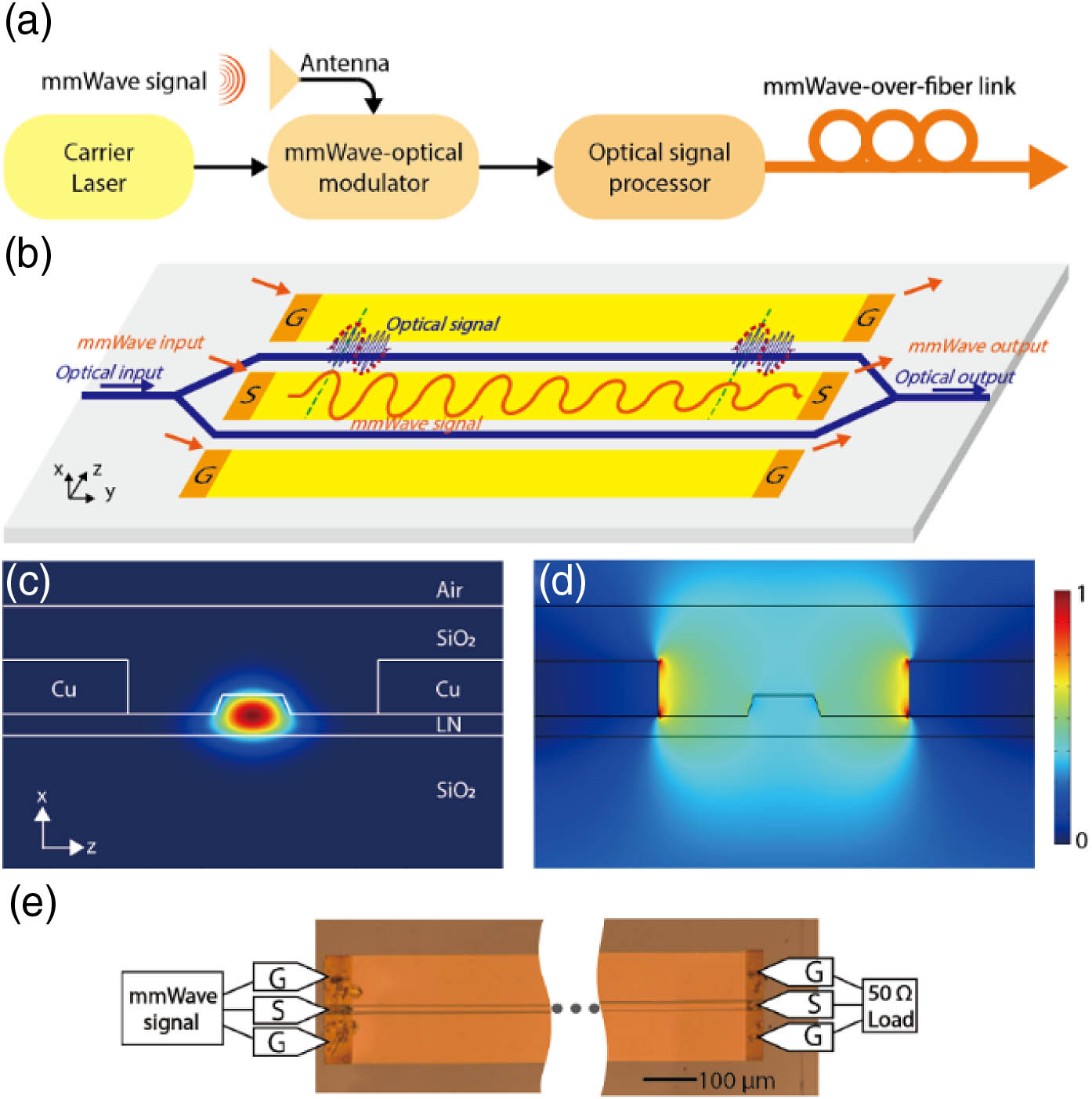
Fig. 1. (a) The schematic illustration of a future mmWave-photonic system, at the heart of which sits the mmWave-optic modulator that converts mmWave signals into the optical domain. (b) The schematic of the TFLN mmWave-optic modulator, where velocity matching between the optical and mmWave signals, impedance matching, and RF loss conditions determine the ultimately achievable modulation bandwidths. (c) The simulated optical mode profile (E z ) in the TFLN rib waveguide. (d) The simulated mmWave profile (E z ) at a frequency of 300 GHz. (e) The optical micrograph of a fabricated device (the darker regions at the two ends are exposed areas for electrical contacts, whereas other parts of the chip are cladded with silicon dioxide).

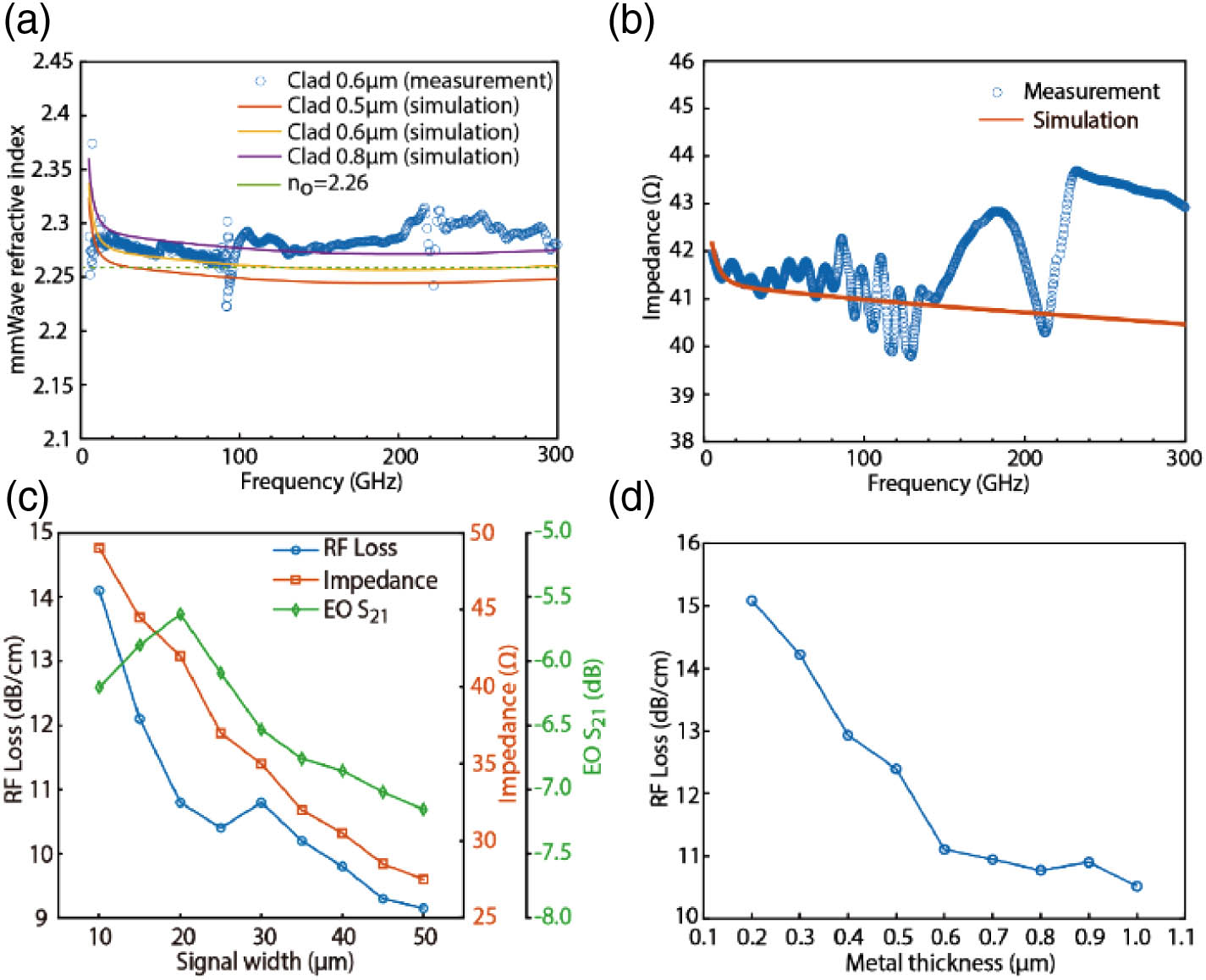
Fig. 2. (a) The simulated mmWave effective (phase) indices for various cladding thicknesses (solid lines), and the actual indices extracted from measured s -parameters (circles) as functions of frequency. The green dashed line shows the simulated optical group index, indicating good velocity matching in the fabricated device. (b) The simulated and extracted characteristic impedance of the device. (c) The simulated RF loss and characteristic impedance, as well as calculated EO S 21 (assuming velocity matching) for various signal widths at 250 GHz, indicating an optimal signal width of 20 μm. (d) The simulated RF loss versus metal thickness at 250 GHz.

Fig. 3. (a) Measured s -parameters of the mmWave transmission lines with lengths of 5.8 and 10.8 mm. (The dashed lines indicate the boundaries of our measurement bands.) (b) Extracted and fitted electrical loss coefficient of the transmission line as a function of frequency.

Fig. 4. (a) Schematic diagram and (b) photo of the measurement setup for characterizing electro-optic responses at frequencies up to 325 GHz.

Fig. 5. (a), (b) Measured and calculated modulator RF V π of the (a) 10.8-mm- and (b) 5.8-mm-devices. (c), (d) Measured and calculated electro-optic responses of the (c) 10.8-mm- and (d) 5.8-mm-devices. Blue circles correspond to the raw measured data directly extracted from the electro-optic sideband measurements. Dashed lines show smoothed values for better comparison with the calculated values. Red lines are calculated based on the n m and Z C values from the measured electrical s -parameters.

Fig. 6. Simulated RF V π versus device length for various velocity- and impedance-mismatch conditions at 250 GHz. The yellow dots correspond to the 5.8-mm- and 10.8-mm-devices in this work. The bottom dashed line corresponds to a capacitive-loaded traveling-wave electrode (CL-TWE), whereas the rest correspond to normal traveling-wave electrodes.

Set citation alerts for the article
Please enter your email address