• Photonics Research
  • Vol. 11, Issue 12, 2128 (2023)
You Xiao1、4、†,*, Xiyuan Cao2、†, Xiaoyu Liu1, Lianxi Jia1, Jia Huang1, Hao Li1、5、*, Aimin Wu1、6、*, Zhen Wang1, and Lixing You1、3
Author Affiliations
  • 1National Key Laboratory of Materials for Integrated Circuits, Shanghai Institute of Microsystem and Information Technology, Chinese Academy of Sciences (SIMIT, CAS), Shanghai 200050, China
  • 2State Key Laboratory of Dynamic Measurement Technology, School of Instrument and Electronics, North University of China, Taiyuan 030051, China
  • 3Center of Materials Science and Optoelectronics Engineering, University of Chinese Academy of Sciences, Beijing 100049, China
  • 4e-mail: xiaoyou@mail.sim.ac.cn
  • 5e-mail: lihao@mail.sim.ac.cn
  • 6e-mail: wuaimin@mail.sim.ac.cn
  • show less
    DOI: 10.1364/PRJ.502849 Cite this Article Set citation alerts
    You Xiao, Xiyuan Cao, Xiaoyu Liu, Lianxi Jia, Jia Huang, Hao Li, Aimin Wu, Zhen Wang, Lixing You. Ultralow-filling-factor superconducting nanowire single-photon detector utilizing a 2D photonic crystal[J]. Photonics Research, 2023, 11(12): 2128 Copy Citation Text show less
    Schematic of (a) top and (b) side views of the structure of ultralow-filling-factor SNSPD (ULFF-SNSPD) integrated with PhC resonator. The NbN nanowire has a width of 80 nm, a thickness of 6 nm, and a period of 650 nm, corresponding to a filling factor of 12.3%. The PhC resonator consists of a Si slab and an array of circular SiO2 cylinders; each cylinder has a radius of 212 nm, a height of 345 nm, and a period of 650 nm. (c) Top and (d) side views of distribution of electric field intensity at 1550 nm for TM-polarized incident light. Absorption, reflection, and transmission of (e) nanowire integrated with PhC resonator and (f) nanowire without PhC resonator at wavelengths of 1450–1650 nm.
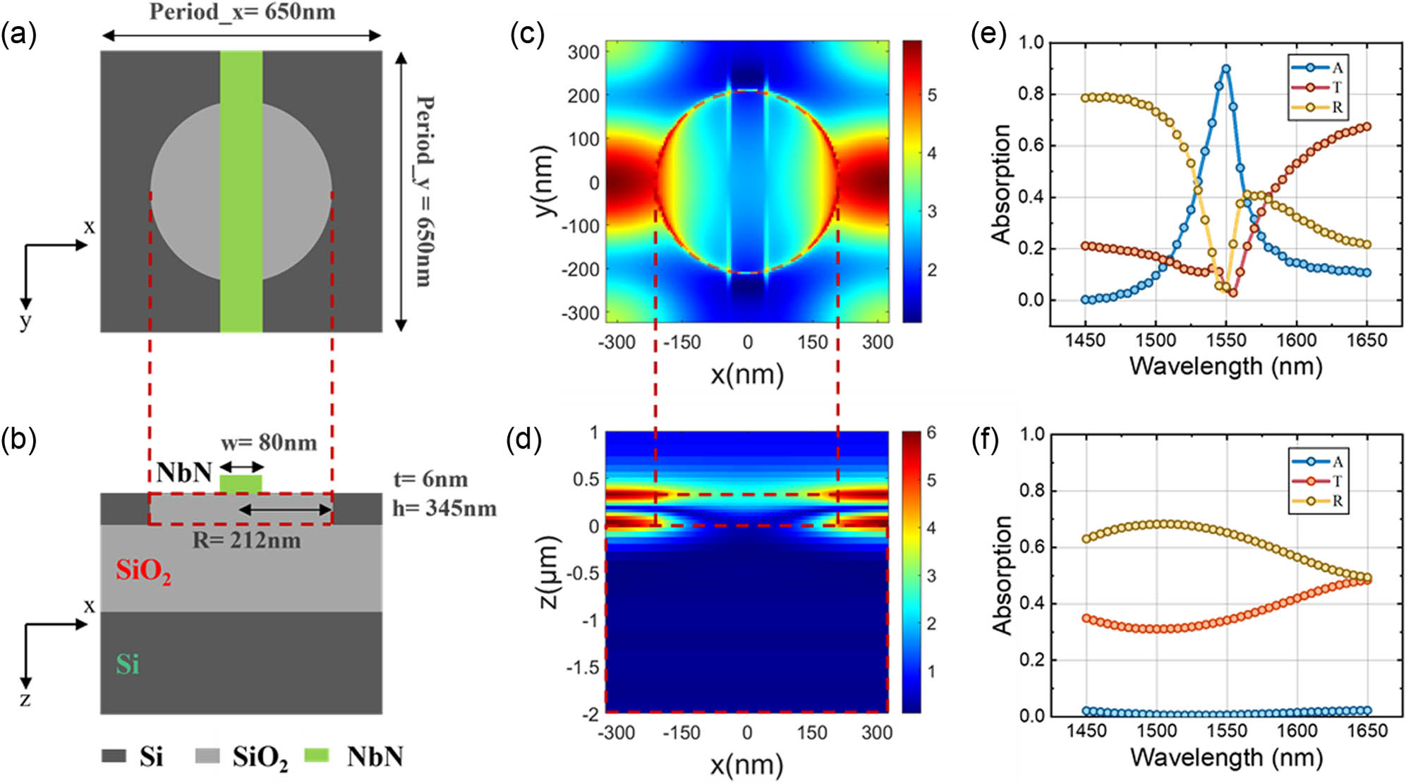
    Fig. 1. Schematic of (a) top and (b) side views of the structure of ultralow-filling-factor SNSPD (ULFF-SNSPD) integrated with PhC resonator. The NbN nanowire has a width of 80 nm, a thickness of 6 nm, and a period of 650 nm, corresponding to a filling factor of 12.3%. The PhC resonator consists of a Si slab and an array of circular SiO2 cylinders; each cylinder has a radius of 212 nm, a height of 345 nm, and a period of 650 nm. (c) Top and (d) side views of distribution of electric field intensity at 1550 nm for TM-polarized incident light. Absorption, reflection, and transmission of (e) nanowire integrated with PhC resonator and (f) nanowire without PhC resonator at wavelengths of 1450–1650 nm.
    (a) Top and (b) side views of distribution of electric field intensity at 1550 nm for TE-polarized incident light. Absorption, reflection, and transmission of (c) nanowire integrated with PhC resonator.
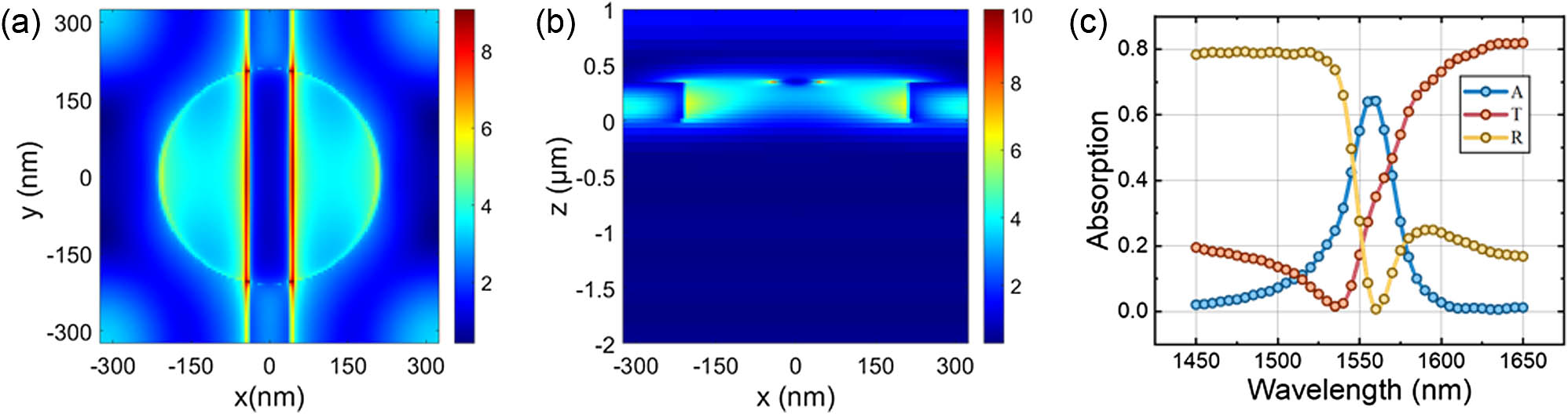
    Fig. 2. (a) Top and (b) side views of distribution of electric field intensity at 1550 nm for TE-polarized incident light. Absorption, reflection, and transmission of (c) nanowire integrated with PhC resonator.
    (a) Absorption spectrum of NbN nanowires as a function of PhC radius and height. The maximum absorption of the design is 90%, reached at a height of 345 nm and a radius of 211 nm. (b) Blue or red shift of absorption peak of NbN nanowires due to PhC radius variation. The absorption peak at a central wavelength of 1550 nm occurs at r=211 nm. (c) PhC height deviation caused by over-CMP effect, resulting in deterioration of absorption of NbN nanowires. The maximum absorption is achieved at h=345 nm. Negligible effect of NbN nanowire (d) thickness variation, (e) width shift, and (f) alignment deviation on absorption.
    Fig. 3. (a) Absorption spectrum of NbN nanowires as a function of PhC radius and height. The maximum absorption of the design is 90%, reached at a height of 345 nm and a radius of 211 nm. (b) Blue or red shift of absorption peak of NbN nanowires due to PhC radius variation. The absorption peak at a central wavelength of 1550 nm occurs at r=211  nm. (c) PhC height deviation caused by over-CMP effect, resulting in deterioration of absorption of NbN nanowires. The maximum absorption is achieved at h=345  nm. Negligible effect of NbN nanowire (d) thickness variation, (e) width shift, and (f) alignment deviation on absorption.
    Fabrication process and characterization of ULFF-SNSPD integrated with PhC resonator. (a) Bottom-up device fabrication: (i) Si hole array etching, (ii) SiO2 filling and CMP, (iii) NbN film sputtering, and (iv) NbN nanowire fabrication. (b) SEM image of a device with meandered structure with 18 μm diameter. Zoomed-in images of (c) photosensitive area and (d) position of NbN nanowire relative to PhC resonator. Nanowires with a width of 85 nm and a period of 640 nm were processed on an array of cylinders with a diameter of 416 nm each and a period of 650 nm each. (e) Cross-sectional SEM image of a cylinder array with etch depth of 343 nm.
    Fig. 4. Fabrication process and characterization of ULFF-SNSPD integrated with PhC resonator. (a) Bottom-up device fabrication: (i) Si hole array etching, (ii) SiO2 filling and CMP, (iii) NbN film sputtering, and (iv) NbN nanowire fabrication. (b) SEM image of a device with meandered structure with 18 μm diameter. Zoomed-in images of (c) photosensitive area and (d) position of NbN nanowire relative to PhC resonator. Nanowires with a width of 85 nm and a period of 640 nm were processed on an array of cylinders with a diameter of 416 nm each and a period of 650 nm each. (e) Cross-sectional SEM image of a cylinder array with etch depth of 343 nm.
    Schematic of broadband continuous spectral scanning system: (a) broadband continuous single-photon light-source module, (b) cryocooler with a minimum working temperature of 2.2 K, and (c) bias and readout components. AOTF, acousto-optic tuning filter; PM, power meter; SMF, single-mode fiber; OS, optical switch. (d) Normalized SDE spectra at 1450–1650 nm, with a peak at 1520 nm. (e) Bias current dependencies of SDE and DCR at 1550 nm. The SDE curve is slightly saturated and peaks at 60% at 15.6 μA.
    Fig. 5. Schematic of broadband continuous spectral scanning system: (a) broadband continuous single-photon light-source module, (b) cryocooler with a minimum working temperature of 2.2 K, and (c) bias and readout components. AOTF, acousto-optic tuning filter; PM, power meter; SMF, single-mode fiber; OS, optical switch. (d) Normalized SDE spectra at 1450–1650 nm, with a peak at 1520 nm. (e) Bias current dependencies of SDE and DCR at 1550 nm. The SDE curve is slightly saturated and peaks at 60% at 15.6 μA.
    (a) Schematic of the side-etching effect. (b) Absorption efficiency of different etching inclination angles. The absorption peak of nanowires is blue shifted as the etching angle increases from 0° to 5°, and the absorption maximum decreases from 90% to 73%. At the same time, the absorption bandwidth gradually becomes broader.
    Fig. 6. (a) Schematic of the side-etching effect. (b) Absorption efficiency of different etching inclination angles. The absorption peak of nanowires is blue shifted as the etching angle increases from 0° to 5°, and the absorption maximum decreases from 90% to 73%. At the same time, the absorption bandwidth gradually becomes broader.
    (a) Normalized response waveforms recorded by the oscilloscope for ultralow-filling-factor (ff=13.8%) device and regular-filling-factor (ff=56.2%) device. The corresponding recovery times (pulse amplitude decline at 1/e) are 12.3 ns and 38.8 ns, respectively, indicating a more than threefold enhancement in detection speed for low-filling-factor structure. (b) Normalized SDE as a function of count rate, which shows a maximum count rate close to 80 MHz under a photosensitive diameter of 18 μm.
    Fig. 7. (a) Normalized response waveforms recorded by the oscilloscope for ultralow-filling-factor (ff=13.8%) device and regular-filling-factor (ff=56.2%) device. The corresponding recovery times (pulse amplitude decline at 1/e) are 12.3 ns and 38.8 ns, respectively, indicating a more than threefold enhancement in detection speed for low-filling-factor structure. (b) Normalized SDE as a function of count rate, which shows a maximum count rate close to 80 MHz under a photosensitive diameter of 18 μm.
     Wavelength (nm)Filling FactorDiameter (μm)tr (ns)SDE at 0.1 MHzSDE at 30 MHzT (K)
    ULFF-SNSPD15100.14181260%36%2.2
    Ref. [23]15500.562182190.5%30%0.85
    Table 1. Detection Performance Comparison
    You Xiao, Xiyuan Cao, Xiaoyu Liu, Lianxi Jia, Jia Huang, Hao Li, Aimin Wu, Zhen Wang, Lixing You. Ultralow-filling-factor superconducting nanowire single-photon detector utilizing a 2D photonic crystal[J]. Photonics Research, 2023, 11(12): 2128
    Download Citation