1National Key Laboratory of Materials for Integrated Circuits, Shanghai Institute of Microsystem and Information Technology, Chinese Academy of Sciences (SIMIT, CAS), Shanghai 200050, China
2State Key Laboratory of Dynamic Measurement Technology, School of Instrument and Electronics, North University of China, Taiyuan 030051, China
3Center of Materials Science and Optoelectronics Engineering, University of Chinese Academy of Sciences, Beijing 100049, China
Superconducting nanowires enable the operation of outstanding single-photon detectors, which are required particularly for quantum information and weak-light measurement applications. However, the trade-off between detection speed and efficiency, which is related to the filling factors of superconducting nanowires, is still a challenge. Here, we propose a fast, efficient single-photon detector fabricated by integrating ultralow-filling-factor meandered superconducting nanowires atop a photonic crystal (PhC) resonator. This unique structure enables a fast photon response due to the low kinetic inductance of the short nanowires and ensures efficient photon absorption due to the resonant effect of the PhC structure. The proposed detector has a filling factor of only while maintaining a high maximum absorption in our simulation of 90%. The fabricated device exhibits a maximum system detection efficiency of 60%, a maximum count rate of , and a recovery time of only , which is three times faster than that of the conventional meandered structure at the same sensing diameter (18 μm). This work helps advance the movement toward high-efficiency, high-speed single-photon detectors and promotes their future application in quantum communication and imaging.
1. INTRODUCTION
The rapid development of superconducting nanowire single-photon detectors (SNSPDs) has enabled numerous applications in diverse frontier fields, such as quantum computing [1], deep-space communication [2], remote sensing [3], and biofluorescence imaging [4]. These fields, particularly LiDAR and imaging, typically require SNSPDs [5] with both high system detection efficiency (SDE) and high speed for better signal-to-noise ratio and maximum count rate (MCR). Usually, ultrathin superconducting films are patterned as meandering nanowires with high filling factors () on distributed Bragg reflectors (DBRs) or metal reflectors to guarantee both saturated-coupling efficiency and absorption efficiency. In these detection scenarios, large-aperture fibers are commonly packaged to receive as many photons as possible, in which case the sensing area of an SNSPD should be enlarged to ensure that all collected photons are coupled into the detector. However, as the sensing area increases, the length of the nanowire grows proportionally, resulting in higher kinetic inductance and, thus, a longer reset time, revealing the trade-off between detection efficiency and detection speed.
Multipixel strategies [6–8] were initially used to overcome this limitation. Multiple SNSPD pixels arranged in arrays or interleaved patterns can greatly reduce each nanowire’s length for a given area, thus significantly increasing the detection speed and MCR without compromising the SDE. Consequently, devices with up to 32 pixels [9] have reached an MCR of 1.5 GHz at a 3 dB compression. Nevertheless, as the pixel number increases, the system readout becomes increasingly complex, and the effects of thermal or electrical cross talk between pixels become nonnegligible. Moreover, various on-chip structures have been introduced to localize the electric field, allowing considerable absorption of short nanowires by increasing the interaction time. Nanowires integrated with waveguides [10–16], micro-ring resonators [17], 1D photonic crystal (PhC) cavities [10,18], and 2D PhC cavities [19] have been developed to realize near-perfect absorption at nanowire lengths as short as 1 μm. However, these structures are more suitable for on-chip detection than direct free-space illumination because of their coupling losses. In addition, a vertical coupling design has been proposed for low-filling-factor nanowires with silicon (Si) slabs and silver (Ag) reflectors [20]. This low-filling-factor strategy can substantially enhance the detection speed without compromising the size of the sensing area. The challenge is to design optical cavity structures to reach high absorption in a fabrication-friendly configuration.
In this work, we develop high-speed, high-efficiency ultralow-filling-factor superconducting nanowires integrated with a PhC resonator. Unlike in other on-chip photonic structures, light is directly illuminated on the nanowires in this setup. The electric field is localized in the PhC resonator and then absorbed by the nanowires above, so high absorption can be achieved even at ultralow filling factors. This addresses the trade-off between detection speed and detection efficiency.
Sign up for Photonics Research TOC. Get the latest issue of Photonics Research delivered right to you!Sign up now
2. METHOD
A. Materials and Design
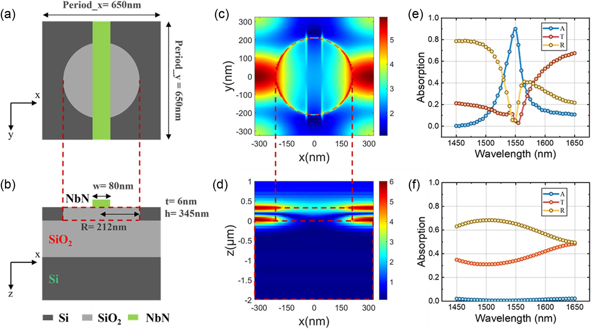
Figures 1(a) and 1(b) illustrate the structure of the proposed ultralow-filling-factor SNSPD (ULFF-SNSPD), which consisted of meandered superconducting nanowires on top of a PhC resonant cavity. The PhC resonant cavity consisted of a Si slab with a cylinder array. The nanowires, each with a width of 80 nm and a thickness of 6 nm, were placed centrally atop the cylinders. A Si-on-insulator (SOI) wafer with a 345-nm-thick top Si layer, a 3-μm-thick layer, and a 400-μm-thick Si substrate was used to process the PhC resonator, whose period was fixed at 650 nm and whose radius was optimized to 212 nm. Niobium nitride (NbN) was selected as the superconducting nanowire for its excellent performance at 2.2 K in a compact Gifford–McMahon cryocooler. Si was used to prepare the PhC resonator because of its high dielectric constant and loss lessness at the target wavelength. The optical constants of Si, , and NbN are 3.46, 1.45, and 5.23–5.82i, respectively. The material dispersion in the observed wavelength range was neglected for simplicity. A simulation was performed using the finite-difference time-domain method. The source was a plane wave with a designed wavelength of 1550 nm at normal incidence, and the electric polarization was along the direction (TM). Boundaries perpendicular to the direction were set as perfect matching layers, and boundaries parallel to the axis were set as periodic boundary conditions. With Si and being transparent in the near-infrared region, light absorption only occurred in the NbN nanowires. The relationship of absorption (), transmission (), and reflection () was expressed as .
Figure 1.Schematic of (a) top and (b) side views of the structure of ultralow-filling-factor SNSPD (ULFF-SNSPD) integrated with PhC resonator. The NbN nanowire has a width of 80 nm, a thickness of 6 nm, and a period of 650 nm, corresponding to a filling factor of 12.3%. The PhC resonator consists of a Si slab and an array of circular cylinders; each cylinder has a radius of 212 nm, a height of 345 nm, and a period of 650 nm. (c) Top and (d) side views of distribution of electric field intensity at 1550 nm for TM-polarized incident light. Absorption, reflection, and transmission of (e) nanowire integrated with PhC resonator and (f) nanowire without PhC resonator at wavelengths of 1450–1650 nm.
Figures 1(c) and 1(d) show the electric field intensity distribution of the structure. The electric field is predominantly localized at the upper and lower interfaces of the PhC, inside the Si slab rather than the cylinder. The high absorption of the nanowire is caused mainly by the effect of this light field localization, which indeed increases the interaction time of the incident light and the nanowires. Although in Fig. 1(c) this part of the energy is confined in the Si slab rather than the region, in this optical system consisting of NbN nanowires and PhC, the superconducting nanowires are the only absorbing material, and the localized light field is finally absorbed by the nanowires through the interactions. The corresponding absorption efficiency is up to 90.0% at 1550 nm, as shown in Fig. 1(e). A structure without a PhC resonator was also analyzed for comparison. The electric fields are reflected into the air or transmitted to the substrate at the same filling factor, resulting in an absorption efficiency as low as 0.6%. By introducing the optimized PhC, we achieve a 150-fold enhancement in the absorption efficiency of the low-filling-factor nanowires. To better understand the effect of this optical cavity, the TM polarization case was also simulated. The results are shown in Fig. 2. While the geometric parameters of this model are kept consistent, in comparison to the incidence case of TM polarization, the electric field is no longer localized in the Si slab for TE polarization but mainly confined at the edges of the superconducting nanowires and the cylinders. The corresponding nanowire absorption under TE polarization is less than 50%, which is lower than 90% under TM polarization, indicating that our device is polarization sensitive.
Figure 2.(a) Top and (b) side views of distribution of electric field intensity at 1550 nm for TE-polarized incident light. Absorption, reflection, and transmission of (c) nanowire integrated with PhC resonator.
In our design, the absorption rate of the nanowires via the external leakage of guided resonances is mostly affected by the PhC radius (), period (), and height (). Considering the fabrication tolerances, we studied the effect of and on absorption. Figure 3(a) indicates that the absorption of the nanowire was crossed at and , corresponding to the maximum value. The variation in the exposure dose during PhC processing can cause radius deviation, resulting in a blue or red shift of the absorption peak. The absorption spectra at , 211 nm, and 216 nm are shown in Fig. 3(b). Within a limited variation of , the absorption peak exhibits a blue shift with an increase in , whereas the maximum absorption fluctuates only slightly. By contrast, the variation of significantly affects the maximum absorption rate. In the fabrication of ultrathin, ultranarrow nanowires on the PhC resonator, the etched holes would be filled with , followed by chemical–mechanical polishing (CMP), which would lead to deviations in the Si thickness. The over-CMP effect, as illustrated in Fig. 3(c), indicates a sharp decay of absorption over the Si thickness.
Figure 3.(a) Absorption spectrum of NbN nanowires as a function of PhC radius and height. The maximum absorption of the design is 90%, reached at a height of 345 nm and a radius of 211 nm. (b) Blue or red shift of absorption peak of NbN nanowires due to PhC radius variation. The absorption peak at a central wavelength of 1550 nm occurs at . (c) PhC height deviation caused by over-CMP effect, resulting in deterioration of absorption of NbN nanowires. The maximum absorption is achieved at . Negligible effect of NbN nanowire (d) thickness variation, (e) width shift, and (f) alignment deviation on absorption.
The processing errors of the superconducting nanowires were also analyzed, including the nanowire thickness (), width (), and alignment deviation (). In our setup, nanowire absorption exhibits a weak correlation in both width and thickness. We simulated the absorption rates at thicknesses of 5.5–7.5 nm and widths of 70–90 nm. As shown in Figs. 3(d) and 3(e), the maximum absorption rate increases from 88.3% to 91.6% with an increase in thickness and rises from 87.8% to 91.4% with an increase in width. Moreover, the nanowires are independent of offset deviation as shown in Fig. 3(f). The shift distance is the horizontal length between the nanowire center and the nearest cylinder center. The absorption rate fluctuates between 90.0% and 92.6% as the shift distance increases from 0 nm to 100 nm.
3. EXPERIMENT
A. Fabrication
Based on the proposed architecture, we fabricated the ULFF-SNSPD integrated with a PhC resonator. The device was fabricated in a bottom-up configuration, as illustrated in Fig. 4(a). First, the PhC resonator was fabricated on a commercial SOI wafer with a top Si thickness of 340 nm () via 193 nm deep-ultraviolet lithography and inductively coupled plasma etching. The active area was approximately μμ, which ensured sufficient alignment tolerance of the NbN sensing area such that almost all the reflected photons were coupled to the nanowires. Then, the circular holes of the PhC resonator were filled with and polished up to the top Si surface via CMP for the deposition of the next film. Then, a 6.5-nm-thick NbN film was deposited on the well-processed PhC substrate at room temperature through reactive DC magnetron sputtering using a mixture of Ar and gases. The nanowire pattern was transferred to the NbN film via electron-beam lithography and reactive ions in a plasma. Finally, an electrode bridge was etched using the reactive ions to form the co-plane waveguide for the readout of electrical signals. Scanning electron microscopy (SEM) was used to characterize the PhC resonator. Figures 3(b)–3(f) show the SEM images of the fabricated device. The SNSPD had a photosensitive diameter of 18 μm, which ensured sufficient optical coupling and absorption. Nanowires with a width of 85 nm and a period of 650 nm were processed on the cylinder array, where each cylinder had a diameter of 416 nm and a period of 650 nm. The cross-sectional SEM image of the cylinder array showed an etch depth of 343 nm.
Figure 4.Fabrication process and characterization of ULFF-SNSPD integrated with PhC resonator. (a) Bottom-up device fabrication: (i) Si hole array etching, (ii) filling and CMP, (iii) NbN film sputtering, and (iv) NbN nanowire fabrication. (b) SEM image of a device with meandered structure with 18 μm diameter. Zoomed-in images of (c) photosensitive area and (d) position of NbN nanowire relative to PhC resonator. Nanowires with a width of 85 nm and a period of 640 nm were processed on an array of cylinders with a diameter of 416 nm each and a period of 650 nm each. (e) Cross-sectional SEM image of a cylinder array with etch depth of 343 nm.
A broadband continuous spectral scanning system was developed to characterize the detection performance of the ULFF-SNSPD; the system consisted of three parts, as illustrated in Figs. 5(a)–5(c). (i) Broadband continuous single-photon light-source module: a broadband supercontinuum source (SC-OEM, YSL Photonics) with an acousto-optic tunable filter (AOTF) was used to output a wavelength sweep of 1350 nm to 1650 nm at 10 nm intervals. The laser was first attenuated to a single-photon level after passing through two cascaded attenuators (81570A, Agilent) and then through a microelectromechanical system optical switch (OSW22-1310E, Thorlabs). One output of the optical switch was connected to an optical power meter (HP81533B with an InGaAs optical head, Agilent) to calibrate the input optical power (), and the other was connected to a polarization controller (FPC561, Thorlabs) and then the detector. The insertion losses () of both ports were calibrated before each spectrum scan to ensure the accurate monitoring of the incident power (). Therefore, the input optical power was expressed as . (ii) Cryocooler: the packaged device was mounted on the cold head of a Gifford–McMahon cryocooler at a working temperature of 2.2 K. (iii) Bias and readout components: this part was connected to the detector through a bias tee and coaxial cables with an impedance of . The bias circuit included an isolated voltage source and a resistor, which provided a quasi-constant current bias to the SNSPD via the DC arm of the bias tee. The voltage pulse generated by the SNSPD was amplified using a room temperature 50 dB low-noise amplifier (LNA-650, RF Bay) with a bandwidth of 30 kHz to 600 MHz and then input into a pulse counter (or oscilloscope).
Figure 5.Schematic of broadband continuous spectral scanning system: (a) broadband continuous single-photon light-source module, (b) cryocooler with a minimum working temperature of 2.2 K, and (c) bias and readout components. AOTF, acousto-optic tuning filter; PM, power meter; SMF, single-mode fiber; OS, optical switch. (d) Normalized SDE spectra at 1450–1650 nm, with a peak at 1520 nm. (e) Bias current dependencies of SDE and DCR at 1550 nm. The SDE curve is slightly saturated and peaks at 60% at 15.6 μA.
The spectral response of the detector could be obtained in a fully automated manner by calibrating the incident power in real time and recording the corresponding count rate at each wavelength. The photon count rate and dark count rate (DCR) could be read out using the pulse counter by switching the attenuator shutters. Thus, the SDE at the studied wavelength sweep was calculated as follows: where () is the Planck’s constant, () is the vacuum speed of light, and is the wavelength of incident light.
C. Detection Performance and Discussion
The spectral response of the device was first evaluated using the setup in Figs. 5(a)–5(c). In the measurement, the ULFF-SNSPD was biased at 90% of the superconducting switching current () to ensure a high SDE and a low DCR. Before scanning the efficiency curve versus wavelength, we adjusted the polarization controller at 1550 nm to ensure maximum absorption. As shown in Fig. 5(d), the SDE curve was normalized to its maximum value, and two peaks were identified at 1480 nm and 1510 nm. The major peak blue shifted from 1550 nm to 1510 nm compared with our design, and the bandwidth was extended. The SDE of the device was then characterized using its SDE and DCR curves over a series of bias currents at the peak wavelength (1510 nm). Before the test, the input optical power was calibrated again, and the polarization controller was adjusted to ensure a maximum count. As seen in Fig. 5(e), the maximum SDE was 60% at 15.6 μA, which was smaller than the simulated maximum absorption of 90%.
Since the 18 μm sensing area could couple most of the photons introduced by the single-mode fiber and the SDE curve was close to saturation, we inferred that the SDE loss was mainly limited by the absorption efficiency, not the coupling and intrinsic efficiency. This could be caused by the following three aspects. First, the uncertainty of the PhC height () during processing, caused by the SOI top silicon thickness error as well as the over-CMP effect. In Fig. 4(e) we see that the actual processed is 343 nm, which is lower than the designed 345 nm. Second is the side-etching effect when fabricating the PhC. In Fig. 4(e) we observe that this angle is about . For this reason, we simulated the effect of different etching inclination angles on the absorption of nanowires. As shown in Fig. 6(b), the absorption peak of nanowires is blue shifted as the etching angle increases from 0° to 5°, and the absorption maximum decreases from 90% to 73%. At the same time, the absorption bandwidth gradually becomes broader, which is consistent with our experimental results in Fig. 5(d). Third is the light divergence introduced by the single mode fiber. This leads to a non-perpendicular incidence and also leads to some interference effects, which affects the absorption efficiency of the nanowire.
Figure 6.(a) Schematic of the side-etching effect. (b) Absorption efficiency of different etching inclination angles. The absorption peak of nanowires is blue shifted as the etching angle increases from 0° to 5°, and the absorption maximum decreases from 90% to 73%. At the same time, the absorption bandwidth gradually becomes broader.
Figure 7.(a) Normalized response waveforms recorded by the oscilloscope for ultralow-filling-factor () device and regular-filling-factor () device. The corresponding recovery times (pulse amplitude decline at ) are 12.3 ns and 38.8 ns, respectively, indicating a more than threefold enhancement in detection speed for low-filling-factor structure. (b) Normalized SDE as a function of count rate, which shows a maximum count rate close to 80 MHz under a photosensitive diameter of 18 μm.
The integration of the PhC resonator into the ULFF-SNSPD overcomes the trade-off between detection efficiency and detection speed. The electric field is localized in the PhC resonator and then absorbed by the nanowires, which increases the design tolerance in terms of the geometry and spatial distribution of the nanowires. Consequently, even superconducting nanowires with ultralow fill factors, small thicknesses, and narrow widths can still achieve high absorption. Notably, the proposed structure requires high PhC processing accuracy. Indeed, the actual absorption efficiency of current devices does depend on the processing accuracy of the diameter, height, and etching steepness of the PhC. We believe that the current 30% loss in SDE compared to the simulation can be optimized by a more accurate processing condition. In the future, the CMP step can be reduced by patterning the nanowires on top of the PhC slab instead of directly above the cylinder array, thus reducing the impact on the uncertainty of the PhC height. In addition to this, an optical film coater can be used to customize amorphous silicon SOI. With the optically monitored coating mode, the coating thickness accuracy can be controlled within 0.3%, which means that at 344 nm, the error is about 1 nm. For reducing the radius uncertainties on the absorption peak shift, a series of photonic crystal arrays with equally spaced diameters can be designed in each batch of fabrication to ensure that the most suitable parameters could be picked. As silicon photonics device processing continues to improve, especially the accuracy of the exposure and etching processes, we are optimistic in realizing such performance shown in the simulations. In addition, multipixel strategy can also be used in this structure to achieve higher speed and SDE simultaneously for very large sensing areas. This will promote future research in the field of LiDAR, imaging, and quantum communication.
4. CONCLUSION
In conclusion, we propose a vertically coupled SNSPD with an ultralow filling factor. Due to the integration of a PhC resonator, the device shows an absorption efficiency of up to 90% at 1550 nm with a filling factor of only . Experimentally, with an 18 μm sensing diameter, the fabricated device achieves a recovery time of 12.3 ns, an MCR close to 80 MHz, and an SDE of 60% at 1520 nm. This work demonstrates the advantages of improving the absorption efficiency of ULFF-SNSPDs, which are expected to be used for applications such as LiDAR, imaging, and quantum communication.
Acknowledgment
Acknowledgment. The authors acknowledge the support from the Superconducting Electronics Facility (SELF) in SIMIT for device fabrication.