
Shi-Wen Xu, Yu-Ming Wei, Rong-Bin Su, Xue-Shi Li, Pei-Nian Huang, Shun-Fa Liu, Xiao-Ying Huang, Ying Yu, Jin Liu, Xue-Hua Wang, "Bright single-photon sources in the telecom band by deterministically coupling single quantum dots to a hybrid circular Bragg resonator," Photonics Res. 10, B1 (2022)
- Photonics Research
- Vol. 10, Issue 8, B1 (2022)
Abstract
1. INTRODUCTION
Telecom-wavelength sources of single photons with high degrees of brightness, purity, and photon indistinguishability are highly desirable for long-distance quantum communication and distributed quantum networks, due to the low photon absorption and small dispersion in silica fibers. In the past decades, telecom-wavelength single-photon sources in a variety of material platforms have been extensively studied, such as atomic sources [1,2], optical nonlinear crystals [3,4], semiconductor quantum dots (QDs) [5–8], defects in silicon carbide [9,10], gallium nitride [11], and carbon nanotubes [12,13]. However, an on-demand telecom-wavelength source of single photons with simultaneous high degrees of brightness, single-photon purity, and photon indistinguishability is still illusive. Atomic ensembles have a long storage lifetime [14], which is good for quantum memory, but their low radiative rates ultimately restrict the brightness of the sources [15]. Spontaneous parametric downconversion (SPDC) sources based on optical nonlinear crystals can be operated at room temperature with high photon indistinguishabilities [16]. However, high single-photon purities can be obtained only with a probability typically
In this work, we present our efforts towards deterministically coupled QD single-photon sources in the telecom wavelength band by positioning single InGaAs QDs into an h-CBR via a wide-field fluorescence imaging technique [37,38]. A Purcell enhancement of 4.2 clearly reveals the efficient coupling between the QDs and h-CBR. We demonstrate an extraction efficiency of
2. EPITAXIAL GROWTH of TELECOM BAND QDs
The samples were grown on semi-insulating GaAs (001) substrates in a solid-state molecular beam epitaxy (MBE) system equipped with a cracker cell for arsenic (As) evaporation and high-energy electron diffraction (RHEED). The deposition temperature was calibrated by the transition temperature
Sign up for Photonics Research TOC. Get the latest issue of Photonics Research delivered right to you!Sign up now
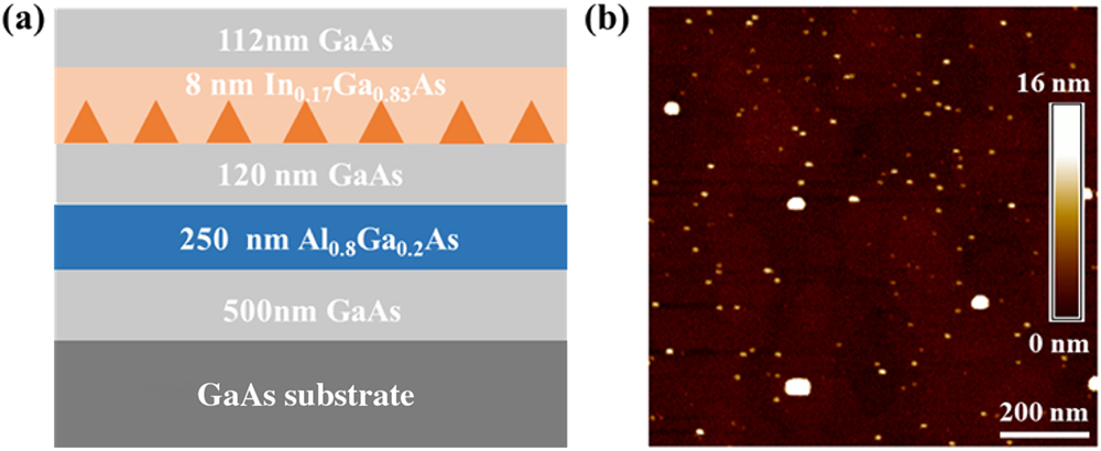
Figure 1.Epitaxial growth of telecom band QDs. (a) Layer sequence of the investigated sample. (b) Representative AFM image of the QDs.
3. CBR DESIGN AND FABRICATION
The
![]()
Figure 2.
4.
A. Coupling between QD and CBR
The h-CBR devices were fabricated in three steps: (i) growing a 300 nm
![]()
Figure 3.Deterministically coupled QD-CBR device. Fluorescence images (
To optically characterize the deterministically coupled devices, a confocal micro-photoluminescence (μ-PL) setup is used. The sample was mounted inside a close-circle cryostat and cooled down to about 4 K. Then a pulsed laser (1150–2323 nm) with a repetition rate of 86 MHz and pulse width of 3 ps or a tunable CW diode laser (1240–1380 nm) was used to excite the QD via one of the excited states (
B. Characteristic of Single-Photon Emission
We investigate the telecom band single-photon emission of our device operating under both CW and pulsed modes for different excitation powers. The single-photon purities of the emitted photons are extracted from the second-order correlations by using a fiber-based Hanbury Brown and Twiss setup. For low-excitation powers of 0.2 μW and 1.1 μW, both CW and pulsed emissions exhibit pronounced suppressions of coincidence events at zero delay, which gives rise to
![]()
Figure 4.Characterizations of the telecom band single-photon emissions. Autocorrelation measurements of single-photon emissions for (a) low-power (0.2 μW) and (b) high-power (4.8 μW) CW excitation. (c) Power dependences of the emission count rate and
Finally, the extraction efficiency of the device at the first lens is evaluated. Figure 5 shows the schematic of the experimental setup. The emitted photons are collected using a microscope objective with an NA of 0.65. For this measurement, the signals pass through a dichroscope and a beam splitter (BS) before coupling into a single-mode fiber. The emitted photons from the targeted emission line are selected by a home-built grating filter and detected by using fiber-coupled SNSPDs. More details are shown in the method section. The detection efficiency of the whole setup has been carefully calibrated to be
![]()
Figure 5.Estimation of the extraction efficiency at the first lens. Left: schematic of the experimental setup (
5. CONCLUSION
In summary, we have demonstrated bright telecom-wavelength single-photon sources based on In(Ga)As/GaAs QDs deterministically coupled to
6. Method
Before fabricating the h-CBR structures, the sample was mounted in a cryostat (Montana) with an internally installed objective (
Acknowledgment
Acknowledgment. We acknowledge the National Super-Computer Center in Guangzhou.
References
[1] T. Chanelière, D. N. Matsukevich, S. D. Jenkins, T. A. B. Kennedy, M. S. Chapman, A. Kuzmich. Quantum telecommunication based on atomic cascade transitions. Phys. Rev. Lett., 96, 093604(2006).
[2] J. Volz, M. Weber, D. Schlenk, W. Rosenfeld, J. Vrana, K. Saucke, C. Kurtsiefer, H. Weinfurter. Observation of entanglement of a single photon with a trapped atom. Phys. Rev. Lett., 96, 030404(2006).
[3] S. Zaske, A. Lenhard, C. A. Keßler, J. Kettler, C. Hepp, C. Arend, R. Al-brecht, W.-M. Schulz, M. Jetter, P. Michler, C. Becher. Visible-to-telecom quantum frequency conversion of light from a single quantum emitter. Phys. Rev. Lett., 109, 147404(2012).
[4] J. H. Weber, B. Kambs, J. Kettler, S. Kern, J. Maisch, H. Vural, M. Jetter, S. L. Portalupi, C. Becher, P. Michler. Two-photon interference in the telecom C-band after frequency conversion of photons from remote quantum emitters. Nat. Nanotechnol., 14, 23-26(2019).
[5] V. Ustinov, N. Maleev, A. Zhukov, A. Kovsh, A. Y. Egorov, A. Lunev, B. Volovik, I. Krestnikov, Y. G. Musikhin, N. Bert, P. S. Kop’ev, Z. I. Alferov, N. N. Ledentsov, D. Bimberg. InAs/InGaAs quantum dot structures on GaAs substrates emitting at 1.3 μm. Appl. Phys. Lett., 74, 2815-2817(1999).
[6] T. Miyazawa, K. Takemoto, Y. Nambu, S. Miki, T. Yamashita, H. Terai, M. Fujiwara, M. Sasaki, Y. Sakuma, M. Takatsu, T. Yamamoto, Y. Arakawa. Single-photon emission at 1.5 μm from an InAs/InP quantum dot with highly suppressed multi-photon emission probabilities. Appl. Phys. Lett., 109, 132106(2016).
[7] B. Alloing, C. Zinoni, V. Zwiller, L. Li, C. Monat, M. Gobet, G. Buchs, A. Fiore, E. Pelucchi, E. Kapon. Growth and characterization of single quantum dots emitting at 1300 nm. Appl. Phys. Lett., 86, 101908(2005).
[8] M. Benyoucef, M. Yacob, J. Reithmaier, J. Kettler, P. Michler. Telecom-wavelength (1.5 μm) single-photon emission from InP-based quantum dots. Appl. Phys. Lett., 103, 162101(2013).
[9] J. Wang, Y. Zhou, Z. Wang, A. Rasmita, J. Yang, X. Li, H. J. von Bardeleben, W. Gao. Bright room temperature single photon source at telecom range in cubic silicon carbide. Nat. Commun., 9, 4106(2018).
[10] L. Spindlberger, A. Csóré, G. Thiering, S. Putz, R. Karhu, J. Hassan, N. Son, T. Fromherz, A. Gali, M. Trupke. Optical properties of vanadium in 4H silicon carbide for quantum technology. Phys. Rev. Appl., 12, 014015(2019).
[11] Z. Mu, A. Rasmita, J. Yang, X. Li, W. Gao. Room-temperature solid-state quantum emitters in the telecom range. Adv. Quantum Technol., 4, 2100076(2021).
[12] X. He, N. F. Hartmann, X. Ma, Y. Kim, R. Ihly, J. L. Blackburn, W. Gao, J. Kono, Y. Yomogida, A. Hirano, T. Tanaka, H. Kataura, H. Htoon, S. K. Doorn. Tunable room-temperature single-photon emission at telecom wavelengths from sp3 defects in carbon nanotubes. Nat. Photonics., 11, 577-582(2017).
[13] X. Ma, N. F. Hartmann, J. K. Baldwin, S. K. Doorn, H. Htoon. Room-temperature single-photon generation from solitary dopants of carbon nanotubes. Nat. Nanotechnol., 10, 671-675(2015).
[14] X.-H. Bao, A. Reingruber, P. Dietrich, J. Rui, A. Dück, T. Strassel, L. Li, N.-L. Liu, B. Zhao, J.-W. Pan. Efficient and long-lived quantum memory with cold atoms inside a ring cavity. Nat. Phys., 8, 517-521(2012).
[15] J. McKeever, A. Boca, A. Boozer, R. Miller, J. Buck, A. Kuzmich, H. Kimble. Deterministic generation of single photons from one atom trapped in a cavity. Science, 303, 1992-1994(2004).
[16] C. I. Osorio, N. Sangouard, R. T. Thew. On the purity and indistinguishability of down-converted photons. J. Phys. B, 46, 055501(2013).
[17] P. Senellart, G. Solomon, A. White. High-performance semiconductor quantum-dot single-photon sources. Nat. Nanotechnol., 12, 1026-1039(2017).
[18] X. Ding, Y. He, Z.-C. Duan, N. Gregersen, M.-C. Chen, S. Unsleber, S. Maier, C. Schneider, M. Kamp, S. Höfling, C.-Y. Lu, J.-W. Pan. On-demand single photons with high extraction efficiency and near-unity indistinguishability from a resonantly driven quantum dot in a micropillar. Phys. Rev. Lett., 116, 020401(2016).
[19] N. Somaschi, V. Giesz, L. De Santis, J. Loredo, M. P. Almeida, G. Hornecker, S. L. Portalupi, T. Grange, C. Anton, J. Demory, C. Gómez, I. Sagnes, N. D. Lanzillotti-Kimura, A. Lemaítre, A. Auffeves, A. G. White, L. Lanco, P. Senellart. Near-optimal single-photon sources in the solid state. Nat. Photonics., 10, 340-345(2016).
[20] Y.-M. He, J. Liu, S. Maier, M. Emmerling, S. Gerhardt, M. Davanço, K. Srinivasan, C. Schneider, S. Höfling. Deterministic implementation of a bright, on-demand single-photon source with near-unity indistinguishability via quantum dot imaging. Optica, 4, 802-808(2017).
[21] S. Liu, Y. Wei, X. Li, Y. Yu, J. Liu, S. Yu, X. Wang. Dual-resonance enhanced quantum light-matter interactions in deterministically coupled quantum-dot-micropillars. Light Sci. Appl., 10, 158(2021).
[22] M. Davanco, M. T. Rakher, D. Schuh, A. Badolato, K. Srinivasan. A circular dielectric grating for vertical extraction of single quantum dot emission. Appl. Phys. Lett., 99, 041102(2011).
[23] J. Liu, R. Su, Y. Wei, B. Yao, S. F. C. da Silva, Y. Yu, J. Iles-Smith, K. Srinivasan, A. Rastelli, J. Li, X. Wang. A solid-state source of strongly entangled photon pairs with high brightness and indistinguishability. Nat. Nanotechnol., 14, 586-593(2019).
[24] B. Chen, Z. He, Z.-J. Liu, Y.-K. Wang, Y.-N. Gao, I. Aharonovich, Z.-Q. Xu, J. Liu. Simultaneously enhanced linear and nonlinear photon generations from WS2 by using dielectric circular Bragg resonators. Nanophotonics, 9, 2587-2592(2020).
[25] N. M. H. Duong, Z.-Q. Xu, M. Kianinia, R. Su, Z. Liu, S. Kim, C. Bradac, T. T. Tran, Y. Wan, L.-J. Li, A. Solntsev, J. Liu, I. Aharonovich. Enhanced emission from WSe2 monolayers coupled to circular Bragg gratings. ACS Photon., 5, 3950-3955(2018).
[26] F. Liu, A. J. Brash, J. O’Hara, L. M. Martins, C. L. Phillips, R. J. Coles, B. Royall, E. Clarke, C. Bentham, N. Prtljaga, I. E. Itskevich, L. R. Wilson, M. S. Skolnick, A. M. Fox. High Purcell factor generation of indistinguishable on-chip single photons. Nat. Nanotechnol., 13, 835-840(2018).
[27] M. Arcari, I. Söllner, A. Javadi, S. Lindskov Hansen, S. Mahmoodian, J. Liu, H. Thyrrestrup, E. H. Lee, J. D. Song, S. Stobbe, P. Lodahl. Near-unity coupling efficiency of a quantum emitter to a photonic crystal waveguide. Phys. Rev. Lett., 113, 093603(2014).
[28] N. Tomm, A. Javadi, N. O. Antoniadis, D. Najer, M. C. Löbl, A. R. Korsch, R. Schott, S. R. Valentin, A. D. Wieck, A. Ludwig, R. J. Warburton. A bright and fast source of coherent single photons. Nat. Nanotechnol., 16, 399-403(2021).
[29] M. Paul, F. Olbrich, J. Höschele, S. Schreier, J. Kettler, S. L. Portalupi, M. Jetter, P. Michler. Single-photon emission at 1.55 μm from MOVPE-grown InAs quantum dots on InGaAs/GaAs metamorphic buffers. Appl. Phys. Lett., 111, 033102(2017).
[30] M. Paul, J. Kettler, K. Zeuner, C. Clausen, M. Jetter, P. Michler. Metal-organic vapor-phase epitaxy-grown ultra-low density InGaAs/GaAs quantum dots exhibiting cascaded single-photon emission at 1.3 μm. Appl. Phys. Lett., 106, 122105(2015).
[31] M. Anderson, T. Müller, J. Skiba-Szymanska, A. B. Krysa, J. Huwer, R. M. Stevenson, J. Heffernan, D. A. Ritchie, A. J. Shields. Coherence in single photon emission from droplet epitaxy and Stranski–Krastanov quantum dots in the telecom C-band. Appl. Phys. Lett., 118, 014003(2021).
[32] A. Musiał, P. Holewa, P. Wyborski, M. Syperek, A. Kors, J. P. Reithmaier, G. Sęk, M. Benyoucef. High-purity triggered single-photon emission from symmetric single InAs/InP quantum dots around the telecom c-band window. Adv. Quantum Technol., 3, 1900082(2020).
[33] S. Kolatschek, C. Nawrath, S. Bauer, J. Huang, J. Fischer, R. Sittig, M. Jetter, S. L. Portalupi, P. Michler. Bright Purcell enhanced single-photon source in the telecom o-band based on a quantum dot in a circular Bragg grating. Nano Lett., 21, 7740-7745(2021).
[34] J.-H. Kim, T. Cai, C. J. Richardson, R. P. Leavitt, E. Waks. Two-photon interference from a bright single-photon source at telecom wavelengths. Optica, 3, 577-584(2016).
[35] C.-M. Lee, M. A. Buyukkaya, S. Harper, S. Aghaeimeibodi, C. J. Richardson, E. Waks. Bright telecom-wavelength single photons based on a tapered nanobeam. Nano Lett., 21, 323-329(2020).
[36] N. Srocka, A. Musiał, P.-I. Schneider, P. Mrowinski, P. Holewa, S. Burger, D. Quandt, A. Strittmatter, S. Rodt, S. Reitzenstein, G. Sęk. Enhanced photon-extraction efficiency from InGaAs/GaAs quantum dots in deterministic photonic structures at 1.3 μm fabricated by
[37] L. Sapienza, M. Davanço, A. Badolato, K. Srinivasan. Nanoscale optical positioning of single quantum dots for bright and pure single-photon emission. Nat. Commun., 6, 7833(2015).
[38] J. Liu, M. I. Davanço, L. Sapienza, K. Konthasinghe, J. V. De Miranda Cardoso, J. D. Song, A. Badolato, K. Srinivasan. Cryogenic photoluminescence imaging system for nanoscale positioning of single quantum emitters. Rev. Sci. Instrum., 88, 023116(2017).
[39] X. Huang, R. Su, J. Yang, M. Rao, J. Liu, Y. Yu, S. Yu. Wafer-scale epitaxial low density InAs/GaAs quantum dot for single photon emitter in three-inch substrate. Nanomaterials, 11, 930(2021).
[40] N. Srocka, P. Mrowinski, J. Große, M. von Helversen, T. Heindel, S. Rodt, S. Reitzenstein. Deterministically fabricated quantum dot single-photon source emitting indistinguishable photons in the telecom o-band. Appl. Phys. Lett., 116, 231104(2020).
[41] B. Yao, R. Su, Y. Wei, Z. Liu, T. Zhao, J. Liu. Design for hybrid circular Bragg gratings for a highly efficient quantum-dot single-photon source. J. Korean Phys. Soc., 73, 1502-1505(2018).
[42] L. Rickert, T. Kupko, S. Rodt, S. Reitzenstein, T. Heindel. Optimized designs for telecom-wavelength quantum light sources based on hybrid circular Bragg gratings. Opt. Express, 27, 36824-36837(2019).
[43] M. Radulaski, M. Widmann, M. Niethammer, J. L. Zhang, S.-Y. Lee, T. Rendler, K. G. Lagoudakis, N. T. Son, E. Janzén, T. Ohshima, J. Wrachtrup, J. Vučković. Scalable quantum photonics with single color centers in silicon carbide. Nano Lett., 17, 1782-1786(2017).
[44] C. Santori, M. Pelton, G. Solomon, Y. Dale, Y. Yamamoto. Triggered single photons from a quantum dot. Phys. Rev. Lett., 86, 1502-1505(2001).
[45] A. V. Kuhlmann, J. Houel, A. Ludwig, L. Greuter, D. Reuter, A. D. Wieck, M. Poggio, R. J. Warburton. Charge noise and spin noise in a semiconductor quantum device. Nat. Phys., 9, 570-575(2013).
[46] A. L. Efros, M. Rosen. Random telegraph signal in the photoluminescence intensity of a single quantum dot. Phys. Rev. Lett., 78, 1110-1113(1997).
[47] A. Barbiero, J. Huwer, J. Skiba-Szymanska, T. Müller, R. M. Stevenson, A. J. Shields. Design study for an efficient semiconductor quantum light source operating in the telecom C-band based on an electrically-driven circular Bragg grating. Opt. Express, 30, 10919-10928(2022).
[48] S. Ji, T. Tajiri, H. Kiyama, A. Oiwa, S. Iwamoto. Design of bull’s-eye optical cavity toward efficient quantum media conversion using gate-defined quantum dot. Jpn. J. Appl. Phys., 60, 102003(2021).
[49] H. Singh, D. Farfurnik, Z. Luo, A. S. Bracker, S. G. Carter, E. Waks. Optical transparency induced by a largely Purcell-enhanced quantum dot in a polarization-degenerate cavity(2021).
[50] C. Nawrath, H. Vural, J. Fischer, R. Schaber, S. Portalupi, M. Jetter, P. Michler. Resonance fluorescence of single In(Ga)As quantum dots emitting in the telecom C-band. Appl. Phys. Lett., 118, 244002(2021).


Set citation alerts for the article
Please enter your email address

© Copyright 2018-2021 | Chinese Laser Press. All Rights Reserved 沪ICP备15018463号-20