Metasurface analogue of the phenomenon of electromagnetically induced transparency (EIT) that is originally observed in atomic gases offers diverse applications for new photonic components such as nonlinear optical units, slow-light devices, and biosensors. The development of functional integrated photonic devices requires an active control of EIT in metasurfaces. We demonstrate a reversible switching of the metasurface-induced transparency in the near-infrared region by incorporating a nonvolatile phase change material, Ge2Sb2Te5, into the metasurface design. This leads to an ultrafast reconfigurable transparency window under an excitation of a nanosecond pulsed laser. The measurement agrees well with both theoretical calculation and finite-difference time-domain numerical simulation. Our work paves the way for dynamic metasurface devices such as reconfigurable slow light and biosensing.
Electromagnetically induced transparency (EIT) originates from a quantum interference occurring in three-level atomic systems.1 It offers a narrowband transparency window within a wide absorption spectrum. Since the first demonstration of EIT in atomic gases,2 its analogues have been discovered in different solid state systems, including metallic plasmonic structures,3–5 optomechanical systems,6 and coupled optical resonators.7 A plasmonic analogue of EIT employs the destructive interaction between a dark and a radiative plasmon mode of contrasting lifetimes.3 Some advantages of the plasmon-induced EIT phenomena include their potential in highly integrated photonic systems8 for enhancing the nonlinear effect,9 slowing light,10 and improving optical biosensing.11 Recently, the plasmonic analogue of EIT using metasurfaces has been utilized for optical buffers,12 biochemical sensors,13,14 and slow-light devices.15,16 Passive approaches toward tuning of metasurface-induced EIT have been demonstrated, such as by changing the geometrical parameters of the metasurfaces.17,18 For a full exploration of the applications mentioned above, it is essential to develop speedy, active control of the EIT response. This can mimic the real atomic EIT systems in which a pumping light is employed to control the populations in both metastable and dipole-allowed states, and consequently the group velocity and dispersion of light. To date, some effort has been dedicated to dynamically tune the metasurface-induced EIT by integrating various active materials in the terahertz regime including silicon,19,20 vanadium dioxide,21 and graphene.22 However, these tuning strategies cannot be extended to the near-infrared (NIR) region since the active materials involved possess a strong Drude contribution to the dielectric function. The NIR region is, however, a technologically important frequency regime with highly prominent applications, such as optical telecommunications and molecular sensing.23–27
Recently, there have been some remarkable research efforts on the demonstration of actively tunable metasurfaces based upon a variety of functional materials, including chalcogenide glass phase change materials (PCMs),28 liquid crystals (LCs),29,30 epsilon-near-zero (ENZ) materials,31,32 silicon,33,34 and vanadium dioxide ().35–38 Particularly, chalcogenide PCMs have attracted increasing attention due to their phase changing properties.28,39,40 The structural rearrangement in PCMs can be triggered by optical41 or electrical42 pulses, enabling optical (e.g., DVD-RW)43 and nonvolatile phase-change random access memory devices.44 Moreover, compared to the other active mediums, such as LCs, ENZ, and , the amorphous (AM)-to-crystalline (CR) state transition in the most investigated PCMs, (GST225), is nonvolatility,45,46 which makes it ideal for tunable metadevices.28,47–57 For example, energy is only required for the state transition process rather than to uphold a particular state, enabling the GST225-based metasurface to be attractive from a green technology standpoint. Notably, the refractive index of the GST225 experiences the largest variation of across the phase change in the NIR region.46 This may lead to the broadest tuning range of the resonant frequency for tunable NIR metasurfaces. Recently, nanostructured GST225 has been designed to obtain specific switching features,58,59 and it was shown that the phase change ratio of GST225 could be engineered via femtosecond pulses.60 Particularly, a few works have numerically illustrated that the chalcogenide metasurfaces may lead to tunable EIT.61–63 Following these theoretical predictions, the concept of tunable EIT was experimentally verified in a very recent work, which showed that a chalcogenide metasurface can be used to obtain a nonreversible switching of EIT via a thermal annealing system.64 These previous works showed the promising potential of chalcogenide PCM in reconfigurable EIT metadevices in the optical region.
In this work, we demonstrate an active EIT metasurface operating in the NIR region by incorporating chalcogenide PCM into the metasurface design. Different from other conventional designs of electromagnetic interactions-based EIT metasurfaces, e.g., split-ring65 and cut wire (CW) resonators,66 our metasurface consists of an array of asymmetric Au crosses atop a GST225 switchable film. The simplicity of this EIT metasurface design is promising for applications in NIR-integrated photonic chips. We experimentally demonstrate that a GST225 AM-to-CR phase change induces a large tuning of the EIT resonance frequency from 1802 to 1957 nm. Both theoretical calculations and numerical simulations attribute this strong tunability to a variation in the damping rate of the dark mode, owing to the changed refractive index of the GST225 layer. With the advantages of fast reversible switching, simple geometry, small footprint, and light weight, our proposed phase-change metasurface opens up avenues for real-time NIR EIT metasurface devices, which may have promising applications in optical telecommunications.
Sign up for Advanced Photonics TOC. Get the latest issue of Advanced Photonics delivered right to you!Sign up now
2 Results and Discussion
2.1 Design and Fabrication
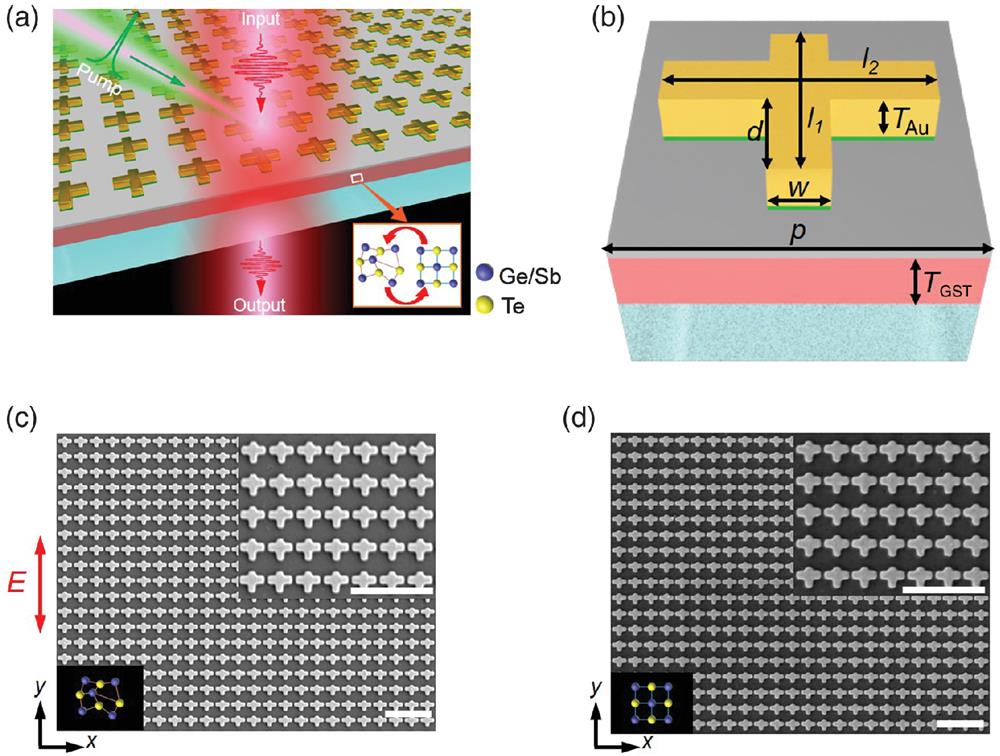
The metasurface consists of arrays of asymmetric Au crosses on a 35-nm thick GST225 phase change film, as shown in Fig. 1(a). Such a meta-atom is simple in geometry and has been rarely reported. This type of metasurface can excite the plasmonic trapped-mode,67,68 where a narrow transparency window can be formed by weakly coupling the excitation mode to the free-space radiation mode.47 The lattice constant of the metasurface is , whereas the lengths of the two arms of the Au cross are and , respectively; the width and height of the two arms are and , respectively [Fig. 1(b)]. To eliminate interlayer diffusion and interfacial reactions, we deposit a 5-nm-thick silicon nitride () diffusion barrier between the Au crosses and the GST225 dielectric layer.69 The geometric parameters enable the phase change metasurface to excite the EIT resonance in the NIR range that covers most optical communication wavelength bands.
Figure 1.Configuration of the EIT metasurface. (a) Schematic of the all-optical, nonvolatile, chalcogenide metamaterial induced EIT switch: single ns laser pulse transits a 35-nm-thick GST225 film, backward and forward between AM and CR on an area covering 510,000 antennae. (b) A representation of the resonator. The geometrical parameters are: , , , , and , respectively; the thicknesses of the top Au resonator and GST225 dielectric layer are and , respectively. The SEM images of the resonators section of the fabricated metasurface (c) before crystallizing and (d) after crystallizing the GST225 dielectric film hybridized with the metasurface. Scale bar: .
In Fig. 1(c), we present a scanning electron microscope (SEM) image of the metasurface sitting on the as-deposited (AD) AM GST255 dielectic layer. We pattern the Au asymmetric crosses array using electron-beam lithography (EBL) followed by Au deposition and a lift-off technique (see Appendix A). The fabrication procedure is schematically shown in Fig. S1 in the Supplementary Material. In the Au asymmetric cross, the vertical cut wire (VCW) with a length of 380 nm works as a super-radiant component that intensely couples with NIR emission polarized along the direction. The horizontal cut wire (HCW), with a length of 550 nm, acts as a subradiant component that weakly interferes with the -polarized incident NIR radiation. However, it is robustly excited by the near-field capacitive coupling with the super-radiant component. The metasurface geometry was optimized to achieve hybrid resonance modes in the NIR spectra. We then crystallize the AD-AM GST225 functional layer by annealing the metasurface for 30 min at 180°C on a thermal hotplate in a flowing Ar atmosphere. In Fig. 1(d), we present that the profile of the antenna can be maintained well as transiting the state of GST225 from AM to CR.
2.2 Experimental Realization of Reversibly Tunable EIT
The GST225 possesses a crystallization temperature of 180°C and a melting temperature of 600°C, and it has been extensively exploited as a platform for robust, speedy, nonvolatile, and reproducible state switching.70–72 Here, the switching between the AM state and crystal state leads to a large change in the complex refractive index (), which subsequently shifts the EIT resonance frequency. In the experiment, the reversible optical switching is triggered by irradiation of ns laser pulses, which induces amorphization and recrystallization of GST225 occurring at different time scales and temperatures.73,74
In Fig. 2(a), we schematically show the phase change metasurface treatment. First, the AD-AM GST225 film is crystallized by annealing the metasurface for 30 min at a crystallization temperature of 180°C on a hotplate in a flowing Ar atmosphere. To reversibly switch GST225 film from the CR to the melt quenched (MQ)-AM state, the crystal lattice needs to be molten and afterward quenched into an AM phase (room temperature) under a rate of to that avoids recrystallizing the atomic structure.75,76 Ultrashort electrical or laser Joule pulses together with a thermally designed structure can offer such a quench rate.77 Electrical switching is widely employed to set and reset phase change random access memory devices; however, it is rarely employed in the transparent NIR metasurfaces due to difficulty in realizing optically transparent electrodes. Herein the ns laser pulse is taken to homogenously convert a 35-nm-thick GST225 film, back and forth, between the AM and CR phases. Specifically, in order to amorphize the CR-GST225 film, a single 5-ns laser pulse with a peak intensity (fluence) of () and a central wavelength of is employed, which is sufficient to increase the local temperature momentarily to above 600°C to melt the GST225. The follow-up fast cooling quenches the melted film into the AM phase. To recrystallize the MQ-AM GST225 film, one lower intensity of () 5-ns laser pulse at is taken to maintain the material above 180°C but below 600°C.
Figure 2.Sequential treatment for the reversible phase transition. (a) Scheme of the reversible phase transition of the GST225 film hybridized with an EIT metasurface: AD-AM GST225 is first annealed above 180°C to change to CR GST225 using a hot plate. A single ns laser pulse (5 ns, ) is triggered to heat the CR GST225 film above 600°C that re-amorphizes the CR GST225. Subsequent quenching results in the MQ-AM GST225. To recrystallise the MQ-AM GST225, for which a temperature above 180°C but below 600°C is required, a single-ns laser pulse with a lower energy (5 ns, ) is taken. (b) Visible–NIR complex refractive index of 35-nm-thick GST225 film at the structural states of the AD-AM (red line), CR (blue line), MQ-AM (orange line), and R-CR (green line), where the refractive index is measured using an ellipsometer over a spectral range of 1000 to 2400 nm.
Figure 2(b) presents the complex refractive index of a 35-nm-thick monolithic GST225 layer for the AD-AM (red line), CR (blue line), MQ-AM (orange line), and recrystalline (R-CR, green line) states. A variable angle spectroscopic ellipsometry (VASE) is used to measure both the real part (, solid lines) and imaginary part (, dashed lines) of the complex refractive index (), which are fitted by a Tauc–Lorentz model. The pronounced change in the between structural states offers the tunability of the NIR resonances of the metasurface. The refractive index variation of GST225 is caused by a bonding transition from predominantly covalent in the AM phase to resonant bonds in the CR phase.39 Note that the spectra of the complex refractive index for AD-AM and MQ-AM GST225, as well as for CR and R-CR GST225, are almost the same, which confirms that the phase change of GST225 is reversible and the material after the short-laser-pulse-induced switching resembles the initial phases after hot-plate thermal annealing.
In Fig. 3(a), we illustrate an all-optical phase change metasurface modulator of EIT operating experimentally at NIR frequencies using a reversible phase transition between the AM and CR in the GST225 film. The transmittance spectra are probed by Fourier transform infrared spectroscopy (FTIR), normalized by that of a bare wafer, the same as the substrate of the metasurface. The normalized transmittance spectrum is split into two panels to distinguish between the metasurface treatments: a comparison between the AD-AM (red solid line) and annealed CR (blue solid line) states is shown in the top panel, and the comparison between the MQ-AM (orange solid line) and the R-CR (green solid line) states after ns laser-induced phase transition is shown in the bottom panel. When the GST225 is in the AD-AM and MQ-AM states, a strong interference between the bright and dark modes leads to an EIT peak between two resonance dips with a transmittance magnitude of 0.5 at . When the GST225 is crystallized by either thermal heating (CR) or laser transition (R-CR), the bright mode dominates and the EIT feature disappears. The CR-GST225 possesses a much higher compared to the AM-GST225 [Fig. 2(b)], which increases the loss to broaden the spectra. This provides a high contrast ratio and modulation depth at . Moreover, the higher of the CR state redshifts the peak resonance. In particular, the peak resonance spectrally moves from to by thermally heating the AD-AM into the CR phase of the GST225 dielectric layer [top panel of Fig. 3(a)]. On the contrary, the changes of the resonant peaks from to and from to are both achieved optically using the ns laser pulse. These variations in the resonant frequency indicate the reversible switching, corresponding to re-amorphization and recrystallization of the GST225 layer, respectively. Namely for the re-amorphization, the CR-GST225 is MQ, shown as a blueshift of the resonant wavelength ( to ). Afterward, the MQ-AM state changes to the R-CR phase again, which is shown as a redshift of the resonant wavelength ( to ). Therefore, the transmittance of the metasurface can transit between two spectrally separate N-IR bands. The active transmittance control and dynamic band-selectivity in the device indicates a main advantage over the previously demonstrated passive infrared photonic metasurfaces.
Figure 3.Experimental realization of reversibly tunable EIT and the comparison with theory and simulation. (a) The FTIR measurement of the normalized transmittance spectra, (b) theoretical fitted transmittance spectra, and (c) numerical simulated transmittance spectra of the phase change metasurface with the different structural states of AD-AM, CR, MQ-AM, and R-CR.
To study the physical origin of the active tuning of the EIT feature, the coupled harmonic Lorentz oscillator model is used to quantitatively analyze the near-field coupling between the VCW (bright mode) and HCW (dark mode) elements in the asymmetric Au cross. It is an analogue of quantum EIT that occurs in atomic systems with three levels. Our theoretical model possesses a ground state and two excited states of and . The bright mode is directly excited by the incident wave polarized along the VCW representing the dipole-allowed transition . The dipole-forbidden transition corresponds to the dark mode in the HCW. By optimizing the metasurface geometry, the dark mode can couple to the bright mode and provide a destructive interaction between paths and . It can suppress the loss strongly and produce a large dispersion within a narrow spectral region. The mode interference in the metasurface is analytically expressed by the coupled Lorentz oscillator model:3,78where , , , and represent the damping rates and amplitudes of the bright and dark resonant modes, respectively. The and are the resonant frequencies of the bright and dark modes, respectively, where is the detuning of the resonant frequency of the dark mode from the bright mode; is the coupling coefficient between the two cutting wires; and is a geometric parameter showing the coupling strength of the bright mode with the incident -field. By solving the coupled Eqs. (1) and (2) with an approximation of , we obtain the susceptibility of the metasurface:79,80
As the energy dissipation is proportional to the imaginary part of susceptibility , we calculate the transmittance by where is the experimental transmittance of the 35-nm GST film on substrate.
In Fig. 3(b), we fit the transmission spectra for the different structural states of the GST225 using Eq. (4), which agrees well with the measurement data [Fig. 3(a)]. The fitting parameters are shown in Table S1 in the Supplementary Material. As is seen, , , and remain unchanged during the reversible phase transition of the GST225 between AM and CR, whereas the damping rate of the dark mode increases by five times the magnitude for the CR state. Therefore, the active tuning of the EIT resonance originates from the variation of . The value of presents the damping of the dark resonant mode and plays a key role in determining the linewidth of the EIT resonance. The of the quadrupole HCW nanoantenna originates almost exclusively from intrinsic losses of the phase change metasurfaces.19,81 In the AM-GST225 based metasurface with a low extinction coefficient () of GST225 [red dashed line in Fig. 2(b)], the two pathways interfere destructively to produce a sharp, EIT-like transmittance peak (red lines in Fig. 3). This is because the low of AM-GST225 can reduce the dielectric losses of the metasurface to minimize , which in turn significantly increases the peak transmittance and quality factor.19 However, as in changing the state of the GST225 layer from AM to CR, the of the GST225 largely increases [blue dashed line in Fig. 2(b)]. This can increase the dielectric loss of the metasurface and obstruct the destructive interaction between the bright and dark modes; thus can be enhanced to completely restrain the excitation of the dark mode and offer a dipole-like transmittance minimum that, in turn, eliminates the EIT resonant peak (blue lines in Fig. 3). For this reason, therefore, the dark mode increases as changing the state of GST225 from AM to CR.
As is seen in Fig. 3(c), the numerically simulated metasurface transmittance spectra are in good agreement with both the measured [Fig. 3(a)] and theoretically fitted [Fig. 3(b)] spectra. A commercial Lumerical Solutions software based on the finite difference time-domain (FDTD) method is carried out to numerically solve Maxwell’s equations for the metasurface. In the model, the refractive index of GST225 film with the different structural states is defined by the measured data in Fig. 2(b). The dielectric constant of Au and substrate is obtained from Palik.82 is defined as a lossless dielectric with a refractive index of .83 The metasurface geometry is the same as that measured by the SEM images presented in Fig. 1(c). A detailed model description is shown in Sec. 2.2. All the simulated spectra are divided by the spectra of the pure substrate. A reversible shift in the resonant peak is observed by switching the state of GST225 between AM and CR. The slight difference between numerical and measured results is possibly due to the presence of native oxides, surface roughness, fabrication imperfections, and a finite acceptance angle of 0.45 NA microscope objectives.
2.3 Resonant Modes in EIT
To explore the fundamental mechanism of the EIT response, we simulated three kinds of phase change metasurfaces based on the AM-GST225 film, which are composed of an Au VCW array [Fig. 4(a)], an Au HCW array [Fig. 4(b)], and a combination of VCW and HCW arrays [Figs. 4(c) and 4(d)]. The VCW antenna array presents a localized surface plasmon resonance (LSPR) at , functioning as a dipolar resonator.3 It thus acts as a radiative or “bright meta-atom” in the EIT metasurface. The resonant wavelength of is more than 5 times larger than the VCW length, having a quality () factor of , calculated by the linewidth of the peak resonance [Fig. 4(a)]. The quality factor is relatively low because of the radiation dissipation, which comprises a large part of the total loss. The HCW resonator acts as the dark meta-atom with a quadrupole surface plasmon resonance (SPR) at . The quadrupole SPR can be viewed as a Fabry–Perot cavity mode with two nodes that travel along the nanorod axis and get reflected at the terminals, as shown in Fig. 4(c). The quadrupole SPR could hardly couple with a normal incidence plane wave, but can be excited with an oblique incidence plane wave or a dipole point source. In other words, it cannot radiate easily and by reciprocity remains dark when illuminated vertically by a plane wave.84–86 So it could serve as a dark mode. Herein, the resonant wavelength of the dark atom is designed to be close to that of the bright (radiative) atom [Fig. 4(b)]. The -factor of the dark meta-atom is , which is about 1 order larger than that of the bright (radiative) mode in magnitude. The metal loss limits the -factor of the dark meta-atom, which may be improved by integrating the gain medium. The strong coupling between the bright and dark resonances results in a sharp transparent peak at in a broad transmittance background [Fig. 4(c)]. The insets in Figs. 4(a) and 4(b) illustrate the -field distributions of the VCW and HCW resonator with the AM-GST225 film, respectively. The HCW is designed to resonate at (dark mode), which is shorter than the resonant wavelength of (bright mode) in the VCW. This guarantees that when the two resonators are coupled together, the resultant bonding resonance at is close enough to the dark mode to permit the resultant resonance to be tuned as changing the coupled resonator system to a single resonator system. In Fig. 4, we show the -field distributions at the EIT-like resonant wavelength of in the metasurface with the AM-GST225 film, and at the LSPR wavelength of in the metasurface with the CR-GST225 film, where the FDTD simulated transmittance spectra for the phase change metasurface are shown in Fig. 3(c). For the AM state, the -field is mainly localized around the two bottom corners of the HCW; however, the -field in the VCW is restrained, which is a typical EIT feature.3 As crystallizing the GST225 dielectric film, the -field in the HCW is significantly suppressed indicating the EIT disappearance. Herein a high -field is formed at the bottom end facets of the VCW due to the LSPR. Therefore, the tuning of EIT resonance originates from the controlling of the dark mode that is achieved by the GST225 phase transition between the AM and CR.
Figure 4.Bright and dark modes in EIT. The FDTD simulated spectra and -field distributions for (a) the VCW resonators array with the AM-GST225 film at , (b) the HCW resonators array with the AM-GST225 film at , (c) the metasurface with the AM-GST225 film at , and (d) the metasurface with the CR-GST225 film at .
The EIT response in the metasurface can lead to a slow-light effect owing to a change of the group velocity () through the device.2 The capability of actively engineering slow light through a device can implement future photonic devices, e.g., slow-light buffers. The of the light propagating in the medium (EIT metasurface) is defined as the inverse of the derived wavenumber () with respect to the angular frequency (): where is the group index. In Fig. 5, we show the dependence of on the wavelength for the metasurfaces with both AM- (red solid line) and CR-GST225 (blue solid line) dielectric films. The metasurface with the AM-GST225 has a maximum negative at , which indicates a slow light effect (small ) owing to the existence of the EIT feature. When switching the GST225 state from AM to CR, however, the is radically reduced since the LSPR dominates. Thus the slow-light effect disappears in the metasurface based on the CR-GST225 film. The is simulated by Lumerical Solutions software. The active controlling of the presented in this work may lead to densely integrated, optically controllable on-chip slow-light devices. Such an EIT metasurface has a large impedance mismatch in the slow-light regime that could be improved using a stack of ultrathin matching layers.87,88
Figure 5.The for the different structural states of the GST225.
To evaluate the repeatability of optical switching of the EIT metasurface, we carried out repeatedly rewritable experiments. Figures 6(a)–6(c) show the experimentally demonstrated transmittance spectra of the metasurface for 30 switching times. As was observed, the metasurface can offer a very robust reconfigurable EIT feature over many times of switching, benefitting from a diffusion barrier between the Au crosses and the GST225 flake. Figure 6(d) shows the peak values of the transmittance for AM (red dots) and CR (blue dots) states with 30 transition times.
Figure 6.(a)–(c) Measured transmittance spectra of the phase change metasurface for 30 switching times. (d) The values of resonance peaks for AM (indicated by red dots) and CR (indicated by blue dots) states with 30 transition times.
We have designed, fabricated, and characterized an all-optical, reconfigurable EIT metasurface for the NIR, achieved by ns laser-induced transiting of the structural state of the chalcogenide semiconductor, GST225. The phase change metasurface offers nonvolatile and active tuning of the resonant mode by switching the state of GST225 between AM and CR. The GST225 phase transition results in a large contrast in its complex refractive index, causing a concomitant resonant wavelength shift of in the NIR spectra. In particular, the phase change metasurface offers an EIT transmittance peak when the state of GST225 film is AM, which can be used to slow the light. However, the EIT response is eliminated and the slow-light effect disappears by crystallizing the GST225 film. These findings may open up a range of innovative applications for slow-light devices, nonlinear devices, and highly sensitive detectors.
4 Appendix: Methods
4.1 Sample Fabrication
-thick silica () wafers are taken as the substrates. Before the deposition, the wafers are washed ultrasonically in acetone, isopropanol, and deionized water and dried by dry nitrogen. The 35-nm-thick GST225 film has been direct current magnetron sputter-deposited on the substrate. A buffer layer with a thickness of 5 nm is deposited on the GST225 layer at a rate from a Si target at a 0.5-Pa pressure. The is attained by reactively sputtering in an atmosphere of 8:2. For nanopatterning the antennae array, EBL (Raith eLINE Plus) with a positive poly(methyl methacrylate) (PMMA) photoresist is used. The EBL-defined patterns are developed using a methyl isobutyl ketone/isopropyl alcohol (MIBK-IPA) 1:3 solution for 60 s. Afterward, a 3-nm-thick Ti layer and a 35-nm-thick Au layer are deposited on the patterned substrates by a fine coater (JEOL JFC-1600AUTO FINE COATER). A lift-off process is carried out using acetone, followed by isopropyl alcohol and a deionized water rinse. The fabricated antenna array is of in size.
4.2 Sample Measurements
The transmittances were measured using an FTIR spectrometer (IFS 66v/S) incorporated with a Bruker IR microscope (Hyperion 2000). The experimental setup can collect data over the infrared region (10,000 to ) with a spectral resolution of . All spectroscopic data are collected in transmission mode through a infrared Schwarzschild objective by a liquid nitrogen-cooled MCT (mercury cadmium telluride) detector. The scanning velocity is 20 kHz. Interferograms are Fourier transformed with a Blackman–Harris three-term apodization and a zero filling factor of 4. Spectral data are obtained using the OPUS 6.0 software. All FTIR spectra collected for metasurfaces are divided by the background spectra of a bare substrate to give a ratio of the transmittance output.
4.3 FDTD Simulations
Simulations are performed by the Lumerical Solutions software based on the FDTD method. The periodic boundary condition is employed in the plane. In the vertical direction ( axis), the simulation area is terminated using perfectly matched layer boundary conditions. The structure is normally illuminated by a plane wave propagating along the direction, and the transmittance is monitored using a power monitor located behind the metasurface. We take a uniform FDTD square mesh () to reduce the numerical error during the FDTD approximation. The numerical models use the tabulated experimental dielectric constants for Au and that take into account the losses. The complex refractive index of GST225 film under different phases is measured by the VASE, which is subsequently fitted using Tauc–Lorentz models.
[23] G. P. Agrawal. Fiber-Optic Communication Systems(2012).
[24] G. P. Agrawal, P. L. Christiansen, M. P. Sorensen, A. C. Scott. Nonlinear fiber optics. Nonlinear Science at the Dawn of the 21st Century, 195-211(2000).