
S. J. Mukhopadhyay, Prajukta Mukherjee, Aritra Acharyya, Monojit Mitra. Influence of self-heating on the millimeter-wave and terahertz performance of MBE grown silicon IMPATT diodes[J]. Journal of Semiconductors, 2020, 41(3): 032103
- Journal of Semiconductors
- Vol. 41, Issue 3, 032103 (2020)
Abstract
1. Introduction
Impact avalanche transit time (IMPATT) oscillators are the most powerful solid state sources for generating microwave (3–30 GHz), mm-wave (30–300 GHz) and terahertz (0.3–10.0 THz) frequencies with sufficiently high power and high DC to RF conversion efficiency[
One major problem with IMPATT oscillators is the self-heating of the diode under reverse bias during oscillating condition, as a result of the high current passing through it. Self-heating of the diode under oscillating condition raises the junction temperature well above room temperature (i.e. T > 300 K). This fact may cause thermal runaway followed by burnout of the device, if the temperature rises beyond the burnout temperature of the base material (which is around TB ≈ 575 K for Si). In order to avoid burnout as a result of self-heating of the diode, it must be mounted on an appropriately designed heat sink made of either metal (copper or silver) or type-IIa diamond[
In the present paper, the authors have studied the influence of junction temperature on both DC and large-signal characteristics of DDR Si IMPATT diodes designed to operate at different mm-wave and THz frequencies. The operating frequencies of DDR Si IMPATT sources chosen for the present study are 94, 140, 220, 300 and 500 GHz. It has already been concluded from the avalanche response time based analysis carried out earlier by the authors that the upper cut-off frequency of DDR Si IMPATT source is around 500 GHz[
2. Structure, material, fabrication and simulation
The descriptions of device structure and corresponding design parameters, material parameters associated with the base semiconductor (i.e. Si), fabrication process and simulation methodology have been presented in this section.
2.1. Structure
The DDR IMPATT diodes possess p+–p–n–n+ structure. The DDR diodes are more powerful and efficient than the single-drift region (SDR) diodes having either n+–n–p+ or p+–p–n+ structure due to the presence of two drift regions in DDR diodes (n- and p-drift regions for the drifting of electrons and holes, respectively) in comparison to the existence of only one drift region in SDR diodes (either n-drift region in n+–n–p+ structure for the drifting of electrons or p-drift region in p+–p–n+ structure for the drifting of holes). As a result of that, DDR diodes are always preferred over SDR diodes, though the fabrication of DDR IMPATT diodes is much more complex. The thickness of p+, p, n, n+ layers (Wp+, Wp, Wn, Wn+) and corresponding doping concentrations (Np+, NA, ND, Nn+) of a diode operating at a particular frequency (fd) are initially chosen using the transit time formula of Sze et al.[
2.2. Material
The electric field and temperature dependences of ionization rate of electrons and holes in Si have been incorporated in the NSVE large-signal simulation program via empirical relations fitted from the experimental data of Grant[
2.3. Fabrication
The (100) oriented n+-type wafers having donor concentration of around ~1025 m–3 can be used as the substrate of mm-wave and THz diodes. Initially the wafer has to be cleaned using RCA etch, followed by Si-beam cleaning at around 850 °C[
2.4. Simulation
The NSVE large-signal simulation technique based on QCDD model has been used to study the effect of junction temperature on both DC and large signal characteristics of DDR Si IMPATT diodes designed to operate at different mm-wave and THz frequencies[
3. Characteristics
It is already reported that DC to RF conversion efficiency of mm-wave and THz DDR Si IMPATT sources are considerably small (< 10%)[
3.1. Static characteristics
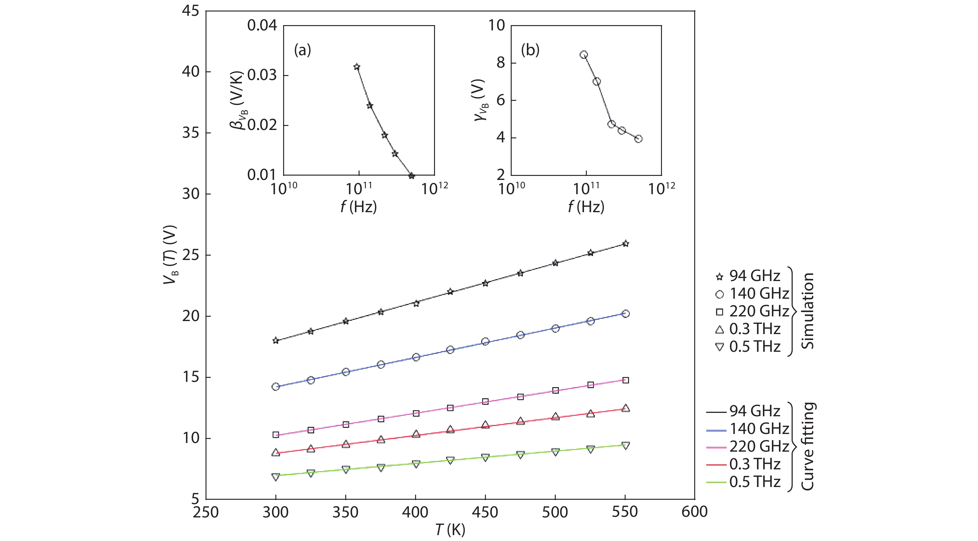
The variations of DC breakdown voltage (VB(T)) of the diodes with temperature have been shown in Fig. 1. The same variations of avalanche zone voltage drop (VA(T)) and avalanche region width (xA(T)) of the diodes are shown in Figs. 2 and 3 respectively. It is interesting to observe from Figs. 1–3 that the said variations of DC parameters with temperature are absolutely linear in nature and all have a positive slope. It is already reported by Grant that the ionization rate of charge carriers in Si decreases significantly with the increase of temperature[
![]()
Figure 1.(Color online) Variations of breakdown voltage of Si IMPATT sources operating at different mm-wave and THz frequencies with temperature; insets of the figure show (a) linear temperature coefficient of breakdown voltage, and (b) corresponding constant linear fitting parameter with operating frequency.
![]()
Figure 2.(Color online) Variations of avalanche zone voltage drop of Si IMPATT sources operating at different mm-wave and THz frequencies with temperature; insets of the figure show (a) linear temperature coefficient of avalanche zone voltage drop and (b) corresponding constant linear fitting parameter with operating frequency.
![]()
Figure 3.(Color online) Variations of avalanche zone width of Si IMPATT sources operating at different mm-wave and THz frequencies with temperature; insets of the figure show (a) linear temperature coefficient of avalanche zone width and (b) corresponding constant linear fitting parameter with operating frequency.
Now, the relations expressing the dependences VB(T), VA(T) and xA(T) with temperature (T) will be formed. It is already observed from Figs. 1–3 that these dependences are linear in nature for all the diodes under consideration. The temperature dependences of a DC parameter can be expressed via the equation of a straight line given by
where
3.2. Large-signal characteristics
The variations of important large-signal parameters such as the avalanche resonance frequency (fa(T)), optimum frequency (fp(T)), peak negative conductance (Gp(T)), corresponding susceptance (Bp(T)), RF power output (PRF(T)) and conversion efficiency (ɳL(T)) of the diodes under consideration with temperature are shown in Figs. 4–9, respectively. All the above variations are observed to be non-linear in nature and can be fitted using a quadratic polynomial equation given by
![]()
Figure 4.(Color online) Variations of avalanche resonance frequency of Si IMPATT sources operating at different mm-wave and THz frequencies with temperature; insets of the figure show (a) quadratic temperature coefficient, (b) linear temperature coefficient of avalanche resonance frequency and (c) corresponding constant fitting parameter with operating frequency.
![]()
Figure 5.(Color online) Variations of optimum frequency of Si IMPATT sources operating at different mm-wave and THz frequencies with temperature; the insets show (a) quadratic temperature coefficient, (b) linear temperature coefficient of optimum frequency and (c) corresponding constant fitting parameter with operating frequency.
where αL = (1/2)(d2L(T)/d2T) is the quadratic temperature coefficient, βL = dL(T)/dT is the linear temperature coefficient of the large-signal
![]()
Figure 6.(Color online) Variations of peak negative conductance of Si IMPATT sources operating at different mm-wave and THz frequencies with temperature; insets of the figure show (a) quadratic temperature coefficient, (b) linear temperature coefficient of peak negative conductance and (c) corresponding constant fitting parameter with operating frequency.
![]()
Figure 7.(Color online) Variations of susceptance corresponding to the peak negative conductance of Si IMPATT sources operating at different mm-wave and THz frequencies with temperature; insets of the figure show (a) quadratic temperature coefficient, (b) linear temperature coefficient of susceptance corresponding to the peak negative conductance and (c) corresponding constant fitting parameter with operating frequency.
![]()
Figure 8.(Color online) Variations of RF power output of Si IMPATT sources operating at different mm-wave and THz frequencies with temperature; insets of the figure show (a) quadratic temperature coefficient, (b) linear temperature coefficient of RF power output and (c) corresponding constant fitting parameter with operating frequency.
The variations of αL, βL and γL associated with all large-signal parameters with the frequency of oscillation have been shown in the insets of the corresponding figures. It is interesting to note that the quadratic temperature coefficients of fa, fp, Gp, PRF and
![]()
Figure 9.(Color online) Variations of DC to RF conversion efficiency of Si IMPATT sources operating at different mm-wave and THz frequencies with temperature; insets of the figure show (a) quadratic temperature coefficient, (b) linear temperature coefficient of DC to RF conversion efficiency and (c) corresponding constant fitting parameter with operating frequency.
3.3. Validation of simulation results
The variations of experimentally measured power output of DDR Si IMPATT sources reported by Luy et al. at 94 GHz, Wollitzer et al. at 140 GHz and Midford et al. at 220 GHz, along with the power output of all mm-wave and THz sources under consideration obtained from simulation with frequency are shown in Fig. 10; all of these experimental measurements and simulations have been carried out near 500 K[
![]()
Figure 10.Variations of RF power output of Si IMPATT sources obtained from the large-signal simulation and experimental measurements[
There are similar studies based on the temperature analysis of DDR IMPATT oscillators based on other semiconductors like some conventional narrow bandgap (NBG) semiconductors such as GaAs, InP, etc. and some wide bandgap (WBG) semiconductors such as 3C-SiC, 4H-SiC, 6H-SiC, Wz-GaN, type-IIb diamond, etc. using similar methodology adopted by the authors to carry out the present work; however, most the important criteria behind this will be the availability of experimentally measured temperature dependent material parameters of the above-mentioned semiconductors. Otherwise, the procedure described in this paper is generic for all base materials mentioned above. Moreover, similar studies can also be carried out for some other IMPATT diode structures like single-drift region (SDR), double-avalanche region (DAR) diodes. Especially, the temperature analysis of low noise DAR Si IMPATT will be very useful for future researchers due to the capability of a single DAR source to operate at multiple bands[
4. Conclusion
The influence of self-heating on the mm-wave and THz performance of DDR Si IMPATT sources has been investigated in this paper. The dependences of static and large-signal parameters on junction temperature are estimated by using a NSVE large-signal simulation technique developed by the authors, which is based on the QCDD model reported earlier. Linear variations of static parameters and non-linear variations of large-signal parameters with temperature have been observed. Analytical expressions representing the temperature dependences of static and large-signal parameters of the diodes are developed using linear and quadratic polynomial curve fitting techniques. These analytical expressions along with the complete set of linear and quadratic temperature coefficients of DC and large-signal parameters calculated and presented in tabular form will be highly useful for designers and researchers to optimize the thermal design of the oscillators. Finally, the simulated results are found to be in close agreement with the experimentally measured data which validates the large-signal results presented in this paper.
References
[1] A Acharyya. Three-terminal graphene nanoribbon tunable avalanche transit time sources for terahertz power generation. Phys Status Solidi A, 216, 1900277(2019).
[2] A Acharyya. 1.0–10.0 THz radiation from graphene nanoribbon based avalanche transit time sources. Phys Status Solidi A, 216, 1800730(2019).
[3] A Biswas, S Sinha, A Acharyya et al. 1.0 THz GaN IMPATT source: effect of parasitic series resistance. J Infrared, Millimeter Terahertz Waves, 39, 954(2018).
[4] A Acharyya. Gallium phosphide IMPATT sources for millimeter-wave applications. Iran J Electr Electron Eng, 14, 143(2018).
[5] T A Midford, R L Bernick. Millimeter Wave CW IMPATT diodes and oscillators. IEEE Trans Microwave Theory Tech, 27, 483(1979).
[6] Y Chang, J M Hellum, J A Paul et al. Millimeter-wave IMPATT sources for communication applications. IEEE MTT-S International Microwave Symposium Digest, 1, 216(1977).
[7] W W Gray, L Kikushima, N P Morentc et al. Applying IMPATT power sources to modern microwave systems. IEEE J Solid-State Circuits, 4, 409(1969).
[8] A Acharyya, J P Banerjee. Prospects of IMPATT devices based on wide bandgap semiconductors as potential terahertz sources. Appl Nanosci, 4, 1(2014).
[9] H Eisele. Selective etching technology for 94 GHz, GaAs IMPATT diodes on diamond heat sinks. Solid State Electron, 32, 253(1989).
[10] M Tschernitz, J Freyer. 140 GHz GaAs double-read IMPATT diodes. Electron Lett, 31, 582(1995).
[11] J J Berenz, F B Fank, T L Hierl. Ion-implanted p–n junction indium-phosphide IMPATT diodes. Electron Lett, 14, 683(1978).
[12] L Yuan, A James, J A Cooper et al. Experimental demonstration of a silicon carbide IMPATT oscillator. IEEE Electron Device Lett, 22, 266(2001).
[13] K V Vassilevski, A V Zorenko, K Zekentes et al. 4H-SiC IMPATT diode fabrication and testing. Technical Digest of International Conference on SiC and Related Materials, 713(2001).
[14] P M Mock, R J Trew. RF performance characteristics of double-drift MM-wave diamond IMPATT diodes. Proc of IEEE/Cornell Conf Advanced Concepts in High-Speed Semiconductor Devices and Circuits, 383(1989).
[15] S Banerjee, A Acharyya, J P Banerjee. Noise performance of heterojunction DDR MITATT devices based on Si~Si1–
[16]
[17] S Banerjee, A Acharyya, M Mitra et al. Large-signal properties of 3C-SiC/Si heterojunction DDR IMPATT devices at terahertz frequencies. Proceedings of the 34th PIERS, 462(2013).
[18] J F Luy, A Casel, W Behr et al. A 90-GHz double-drift IMPATT diode made with Si MBE. IEEE Trans Electron Devices, 34, 1084(1987).
[19] C Dalle, P Rolland, G Lieti. Flat doping profile double-drift silicon IMPATT for reliable CW high power high-efficiency generation in the 94-GHz window. IEEE Trans Electron Devices, 37, 227(1990).
[20] M Wollitzer, J Buchler, F Schafflr et al. D-band Si-IMPATT diodes with 300 mW CW output power at 140 GHz. Electron Lett, 32, 122(1996).
[21] A Acharyya, J Chakraborty, K Das et al. Large-signal characterization of DDR silicon IMPATTs operating up to 0.5 THz. Int J Microwave Wireless Technol, 5, 567(2013).
[22] A Acharyya, S Banerjee, J P Banerjee. Effect of junction temperature on the large-signal properties of a 94 GHz silicon based double-drift region impact avalanche transit time device. J Semicond, 34, 024001(2013).
[23] A Acharyya, J Goswami, S Banerjee et al. Quantum corrected drift-diffusion model for terahertz IMPATTs based on different semiconductors. J Comput Electron, 14, 309(2015).
[24] S M Sze, R M Ryder. Microwave avalanche diodes. Proc IEEE, 59, 1140(1971).
[25] W N Grant. Electron and hole ionization rates in epitaxial silicon at high electric fields. Solid State Electron, 16, 1189(1973).
[26] C Canali, G Ottaviani, A A Quaranta. Drift velocity of electrons and holes and associated anisotropic effects in silicon. J Phys Chem Solids, 32, 1707(1971).
[27]
[28]
[29] Y P Varshini. Temperature dependence of the energy gap in semiconductors. Physica, 34, 149(1967).
[30] W Kern, D A Puotinen. Cleaning solutions based on hydrogen peroxide for use in silicon semiconductor technology. RCA Rev, 31, 187(1970).
[31] K Kugimiya, Y Hirofuji, N Matsuo. Si-beam radiation cleaning in molecular-beam epitaxy. Jpn J Appl Phys, 24, 564(1985).
[32] H Jorke, H Kibbel. Doping by secondary implantation. J Electrochem Soc, 133, 774(1986).
[33] S S Iyer, R A Metzger, F G Allen. Sharp profiles with high and low doping levels in silicon growth by molecular beam epitaxy. J Appl Phys, 52, 5608(1981).
[34] U Koenig, H J Herzog, H Jorke et al. Si-MBE with a high throughput of large diameter wafers. 2nd Int Symp MBE and Related Clean Surface Techniques (Tokyo), 193(1982).
[35] A Casel, H Jorke, E Kasper et al. Dependence of hole transport on Ga doping in Si molecular beam epitaxial layers. Appl Phys Lett, 48, 922(1986).
[36] A Acharyya, S Chatterjee, J Goswami et al. Quantum drift-diffusion model for IMPATT devices. J Comput Electron, 13, 739(2014).
[37] A Acharyya, M Mukherjee, J P Banerjee. Effects of tunnelling current on mm-wave IMPATT devices. Int J Electron, 102, 1429(2015).
[38] A Acharyya, S Ghosh. Dark current reduction in nano-avalanche photodiodes by incorporating multiple quantum barriers. Int J Electron, 104, 1957(2017).
[39] G N Dash, S P Pati. Small-signal computer simulation of IMPATT diodes including carrier diffusion. Semicond Sci Technol, 6, 348(1991).
[40] A Acharyya, S Banerjee, J P Banerjee. Influence of skin effect on the series resistance of millimeter-wave of IMPATT devices. J Comput Electron, 12, 511(2013).
[41] A Acharyya, S Banerjee, J P Banerjee. A proposed simulation technique to study the series resistance and related millimeter-wave properties of Ka-band Si IMPATTs from the electric field snap-shots. Int J Microwave Wireless Technol, 5, 91(2013).
[42] A M Bandyopadhyay, A Acharyya, J P Banerjee. Multiple-band large-signal characterization of millimeter-wave double avalanche region transit time diode. J Comput Electron, 13, 769(2014).

Set citation alerts for the article
Please enter your email address
© Copyright 2018-2021 | Chinese Laser Press. All Rights Reserved 沪ICP备15018463号-20