Shun-Xin Li, Jia-Cheng Feng, Yang An, Hong Xia, "Flexible, self-powered, and polarization-sensitive photodetector based on perovskite lateral heterojunction microwire arrays," Photonics Res. 11, 2231 (2023)
Copy Citation Text
The fabrication of different perovskite materials with superior properties into lateral heterostructures can greatly improve device performance and polarization sensitivity. However, the sensitivity of perovskites to solvents and environmental factors makes the fabrication of lateral heterojunctions difficult. Here, we realize high-quality perovskite microwire crystal heterojunction arrays using regioselective ion exchange. Photodetectors with responsivity and detectivity up to and Jones are fabricated. The photodetector exhibits responsivity as high as at 0 V bias. In addition, the device exhibits ultra-high polarization sensitivity with a dichroic ratio of 5.6, and 81% of its performance was maintained after 144 days of exposure to air.
1. INTRODUCTION
As an important component of integrated optoelectronics, the application of photodetectors has expanded from traditional sensing, communication, and imaging to new emerging fields such as flexible robotics and artificial intelligence [1–6]. The expanding application scenarios have more requirements on photodetectors such as low cost, high performance, and flexibility [7–13]. In particular, the self-powered capability of photodetectors and their sensitivity to other information such as polarization are particularly important for some new application scenarios [14,15]. However, photodetectors based on single-component active layers can hardly meet all these requirements at the same time [16–18]. In contrast, careful construction of materials with different optoelectronic properties into heterostructures is a very effective means to achieve photodetectors with multiple advantages [2,19–21].
Compared to vertical heterojunctions, planar lateral heterostructures avoid light loss at multilayer interfaces and have the advantage of easy integration [22]. However, many emerging optoelectronic materials, such as organic–inorganic hybrid perovskites, are difficult to be prepared as lateral heterojunctions due to complex preparation processes [2]. Although heterostructures of organic–inorganic hybrid perovskites and other materials have achieved a variety of high-performance photodetectors and are widely used in imaging, detection, and sensing applications [23–25], it is still challenging to perfectly “stitch” two organic–inorganic hybrid perovskites into a lateral heterostructure [26,27]. The preparation of lateral heterojunctions for conventional inorganic semiconductors is difficult to be directly applied to solvent- and environment-sensitive organic–inorganic hybrid perovskites [2]. For example, Zhao et al. realized the preparation of high-quality transverse heterostructures by using ion exchange instead of the traditional solution spin coating method [20]. Moreover, in the process of preparing lateral heterojunctions by the solution method, the material deposited first is easily dissolved by the subsequent solvent [28]. In addition, the large number of grain boundaries and defects in perovskite films not only degrades the performance of the device, but also degrades the device stability [29]. Therefore, it is very important to develop a lateral heterojunction fabrication method suitable for two organic–inorganic hybrid perovskite materials with high-crystal quality for realizing high-performance and stable photodetectors [20].
Here, we propose a nanoimprint-assisted preparation of perovskite microwire crystals combined with ion exchange to fabricate lateral heterostructures and achieve high-performance photodetectors with high polarization sensitivity and environmental stability. After obtaining high-quality perovskite microwire crystals by nanoimprinting, the preparation of high-quality perovskite–perovskite heterojunctions is simply achieved by anion exchange. Benefiting from the high crystal quality and perfect heterojunction interface, the fabricated photodetectors exhibit high performance and outstanding environmental stability. Under a bias of 5 V, the photodetector showed responsivity, detectivity, EQE, and LDR as high as , Jones, 254,187%, and 121 dB, respectively. The photodetector exhibits responsivity and detectivity up to and Jones under a self-powered condition. Furthermore, the heterojunction endows the device with a high polarization sensitivity of a high dichroic ratio up to 5.6. The device retains 78% of its original performance after 3000 bending cycles. Device performance retains up to 81% after 144 days in air. These results provide ideas for designing high-performance photodetectors.
Sign up for Photonics Research TOC. Get the latest issue of Photonics Research delivered right to you!Sign up now
2. RESULTS AND DISCUSSION
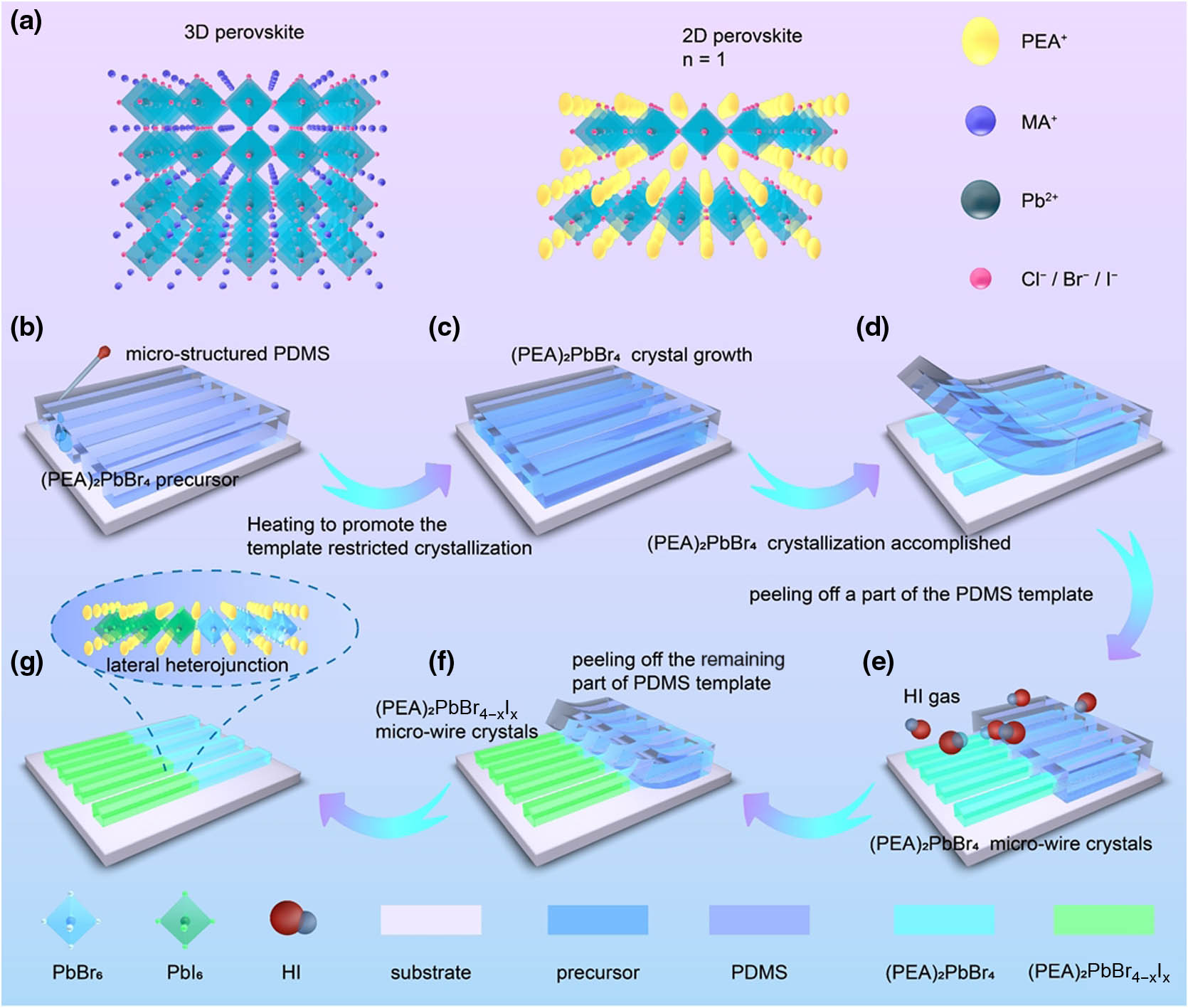
The quantum well structure of a 2D Ruddlesden–Popper type perovskite endows it with unique optoelectronic properties, and the substitution of large cations for smaller radius cations enables better stability. Especially when , the unique 2D layered structure endows it with properties like 2D materials. The long hydrophobic organic chain protects the regular octahedral structure of , which greatly improves its stability compared with 3D perovskites. Therefore, in this work, with was chosen to fabricate a lateral heterojunction [Fig. 1(a)].
Figure 1.(a) Schematic diagram of 3D perovskite and 2D Ruddlesden–Popper perovskite structures; (b)–(d) schematic diagram of process for preparing microwire crystals by imprinting; (e)–(g) regioselective ion exchange preparation of lateral heterojunction.
High-quality micro/nano-crystals with ordered orientation and suppressed grain boundaries and defects are important for high-performance optoelectronic devices. Here, highly aligned microwire crystals were first fabricated to serve as platforms for the construction of heterojunctions. The confinement of the flow direction and location of the perovskite precursor solution by nanoimprinting ensures the quality and order of the crystals. As shown in Figs. 1(b) and 1(c), the non-interfering micro-channel array formed by the PDMS template [Appendix A, Fig. 7(a)] and the substrate restricted the flow direction and position of the precursor solution. After the solvent has gradually evaporated completely, the independent liquid strip arrays are transformed into mutually independent microwire crystal arrays. The as-prepared microwires are not only highly aligned, but also have a smooth surface, which demonstrates their high crystal quality and is beneficial for carrier separation and transport [Appendix A, Fig. 7(b)]. The high crystal quality and order are further demonstrated by the sharp and clear blue fluorescence in the fluorescence micrographs [Appendix A, Fig. 7(c)]. The PDMS template is in close contact with the glass substrate, forming separate channels, and the flow of the solution is restricted within the micrometer-scale one-dimensional channels instead of flowing in arbitrary directions. Therefore, the obtained crystal morphology is still limited by the template and exhibits a layered structure in the direction perpendicular to the substrate [Appendix A, Fig. 7(d)].
The fabrication of high-quality heterojunctions is achieved simply by anion exchange, taking advantage of the reconfigurable anionic bonds of perovskites. To achieve regioselective anion exchange, one half of the PDMS was torn off so that the high-quality microwires were exposed, and the other half was left on the crystal to avoid anion exchange [Fig. 1(d)]. Subsequently, this system was exposed to HI atmosphere [Fig. 1(e)]. With the increase of exposure time, Br in crystals exposed to HI atmosphere was gradually replaced by I to form , while the crystals protected by PDMS showed no change in composition. After the anion exchange process was completed, the other half of the PDMS film was peeled off to obtain high-quality and highly ordered lateral heterojunction arrays with clear interfaces [Figs. 1(f) and 1(g)].
The SEM image of the heterojunction shows a clear interface of the lateral heterojunction array [Fig. 2(a)]. The interface and the distribution of elements near the interface were further analyzed by EDS [Fig. 2(b)]. At the end exposed to HI, the Br element in the microwire is greatly reduced, which indicates that a large amount of the Br element is replaced by the I element. At the end protected by PDMS, the distribution of Br elements on the microwires is obviously more than that on the exposed end, indicating that PDMS plays a role in preventing ion exchange for the microwire crystals. Fluorescence microscopy images clearly demonstrated the fluorescence distribution at different positions of the heterojunction [Figs. 2(c)–2(e)]. The bright blue fluorescence in Fig. 2(c) represents the at the end without ion exchange. The green distribution in Fig. 2(d) represents the microwire crystals produced after ion exchange. The two components have a clear boundary, effectively forming a perfectly stitched lateral heterojunction structure [Fig. 2(e)], which is very beneficial for the realization of high-performance devices. The absorption spectrum of Fig. 2(f) shows that the heterojunction possesses both and absorption peaks. In addition, the XRD pattern shows that has the same diffraction pattern as . This indicates that the ion exchange process did not destroy the crystal structure of microwire crystals [Fig. 2(g)]. Comparing the Raman spectra of , , and , it is found that has Raman peaks of both and [Fig. 2(h)]. Unstable ion gradients can lead to ion migration, compositional mixing, or structural disorder, thereby reducing the material’s stability and shortening its lifespan. Therefore, we have evaluated and characterized the stability of the compositional gradient following the ion exchange process. First, we conducted EDS analysis on the heterojunction stored for 7 days to examine the spatial distribution of elements along the compositional gradient [Appendix B, Figs. 8(a) and 8(b)]. Compared to the initial state, there was no significant change in the element distribution gradient of the heterojunction after 7 days, indicating a slow ion migration process and relative stability of the heterojunction. On the other hand, we characterized the fluorescence distribution of the heterojunction after 7 days of storage. In contrast to EDS analysis, the fluorescent image can more clearly demonstrate ion migration by displaying different colors corresponding to crystal luminescence, thus providing a more intuitive representation of the elemental composition gradient. The fluorescence images showed that the boundary between the blue and green regions of the sample after 7 days was less sharp compared to the initially well-defined fluorescence distribution [Appendix B, Figs. 8(c)–8(e)], indicating a slight change in the compositional gradient due to ion migration.
Figure 2.(a) SEM image of the lateral heterojunction array; (b) I, Pb, Br element distribution of lateral heterojunction; (c)–(e) fluorescence microscope photos of lateral heterojunction array; (f) absorption spectrum, (g) XRD pattern, and (h) Raman spectrum of , , and ; (i) typical time-resolved photoluminescence curves of and .
The time-resolved fluorescence curve is shown in Fig. 2(i). Through double exponential fitting, it is found that the micro-wire crystal has a nanosecond fluorescence lifetime, suggesting that the heterojunction structure of the micro-wire crystal can well separate the photogenerated carriers and promote the formation of photocurrent. A slight decrease in lifetime after iodide ion exchange has been observed. We speculate that several factors contribute to this phenomenon, including the introduction of water-based HI during the ion exchange process. The decrease in lifetime may be attributed to a combination of factors related to the chemical and physical changes induced by the ion exchange process. Firstly, water content present in the HI solution used for ion exchange can lead to increased moisture absorption by the perovskite crystal. This moisture absorption can cause degradation of the perovskite material, leading to a decrease in carrier lifetime. Furthermore, the ion exchange process itself introduces structural modifications in the perovskite film. During the exchange, iodide ions are substituted with other anions from the HI solution, altering the composition and crystal structure of the perovskite microwires. These changes can result in defects, trap states, and non-radiative recombination sites within the perovskite material, thereby reducing the lifetime of charge carriers and excitons. In addition to these factors, the presence of impurities or contaminants in the HI solution can also contribute to the decreased lifetime. It is essential to ensure the purity and quality of the HI solution to minimize any adverse effects on the perovskite film. Therefore, the decrease in lifetime observed after iodide ion exchange may be a result of multiple factors, including moisture absorption, structural modifications, and impurities introduced during the ion exchange process.
In order to further understand the carrier dynamics in the microwire crystal and the microwire crystal after ion exchange, we have carried out a femtosecond transient absorption test on the microwire crystal before and after ion exchange (Fig. 3), and the excitation wavelength is 365 nm. The TA spectra of these two samples have obvious ground state bleaching peaks. For the sample without ion exchange, the ground state bleaching peak is at 405 nm [Figs. 3(a) and 3(b)]. After ion exchange [Figs. 3(d) and 3(e)], the ground state bleaching peak is located at 518 nm, which is close to the steady-state absorption peak of , indicating that after ion exchange, the characteristics of the microwire crystal are closer to . The dynamic process of the excited state is also analyzed, as shown in Figs. 3(c) and 3(f). With double exponential fitting, it is found that both samples have long carrier lifetimes, which is due to the improvement of crystal quality benefitting from the limiting effect of the micron channel on the crystal process. The above results show that the prepared lateral heterostructure is conducive to the separation and transport of carriers, and is very suitable for high-performance optoelectronic devices.
Figure 3.(a) Color plot of TA spectra from ; (b) TA spectra at 398–410 nm; (c) TA kinetics probed at a selected wavelength of 405 nm from (a); (d) color plot of TA spectra from ; (e) TA spectra at 498–545 nm; (f) TA kinetics probed at a selected wavelength of 518.9 nm from (d).
A lateral photoconductive photodetector has been fabricated based on this lateral heterojunction array [Fig. 4(a)]. In this lateral structure, the light is directly irradiated on heterojunctions, avoiding the reflection loss at the interfaces of the multilayer thin film in the vertical structure. Under different bias voltages, the photocurrent of the device increases with the increase of bias voltage. This is because a large bias voltage can separate more photogenerated carriers and thus generate a stronger photocurrent [Fig. 4(b)].
Figure 4.(a) Sketch of a lateral heterojunction photodetector based on ; (b) I-V curve of PD under different light intensities; (c) I-t curve of the PD under different intensities of on–off light irradiation and 5 V bias; (d) variation of photocurrent and with light intensity under 5 V bias; (e) I-t curve of PD under different on–off light intensities and 0 V bias; (f) under 0 V bias, the photocurrent and versus light intensity.
Under 5 V bias, the increases with the enhancement of incident light intensity , indicating that more carriers are generated under strong light [Figs. 4(c) and 4(d)]. In the absence of any light, the current of the PD is as low as 0.3 nA [Appendix C, Fig. 9(a)], illustrating that the high crystal quality suppresses defects and grain boundaries. , an important parameter for evaluating PD performance levels, is calculated up to () according to the following formula:
Two other parameters for evaluating PD performance, detectivity and EQE, are up to Jones and 254,187%, respectively, according to the following formulas [Appendix C, Fig. 9(b)]: where is the device area, is Planck’s constant, is the speed of light, is the electron charge, and is the wavelength of detected light. LDR, a variation range that characterizes the optical signal detected by the PD without distortion, is calculated according to the following formula: where the and are the strongest and weakest light intensities that the PD can detect. The LDR of the PD is as high as 121 dB when operating at 5 V bias. The performance of this lateral heterojunction photodetector in the self-powered situation was further explored. As shown in Fig. 4(e), with the enhancement of , the increases significantly, proving that the built-in electric field at the heterojunction can effectively separate many photogenerated carriers without any external bias. At 0 V bias, the dark current of the PD is as low as 7 pA owing to the suppressed carrier trap state [Appendix C, Fig. 9(c)]. Figure 4(f) shows the dependence of and on light intensity under a self-powered condition. Even without external bias, is as high as . The D and EQE of the PD are as high as Jones and 4921%, respectively [Appendix C, Fig. 9(d)]. The above results demonstrate the high crystal quality of the prepared heterojunction, which facilitates the separation and transport of photogenerated carriers. The performance of this lateral heterojunction-based photodetector is outstanding compared to previously reported results (Table 1).
Performance of Perovskite–Perovskite Heterojunction-Based Photodetectors
Materials
(nm)
(Jones)
Flexible
Long-Term Stability
Reference
460
8.12 at 30 V
No
NA
[1]
405
0.39 at 1 V
No
NA
[30]
650
0.125 at 0 V
NA
90% after 500 bending cycles
85% after 15 days
[2]
500
at 5 V
NA
No
NA
[31]
405
0.444 at 0 V 3.463 at 1.5 V
9000 bending cycles
NA
[32]
405
No
No obvious change after 40 days
[33]
2D/3D perovskite
532
at 2 V
NA
No
71% after 30 days
[34]
405
at 0 V
No
Negligible degradation after 30 days
[19]
532
265 at 5 V
NA
No
90% after 10 days
[20]
365
748 at 5 V 13.5 at 0 V
at 5 Vat 0 V
78% after 3000 bending cycles
81% after 144 days
This study
With the continuous expansion of the application scope of PDs, emerging application scenarios have higher and higher requirements for PDs to detect other properties of light, such as polarization information of light. Although the highly anisotropic structures are beneficial to the improvement of the polarization sensitivity of perovskite photodetectors, their polarization sensitivity is limited by the isotropic characteristics of the photoelectric properties of perovskite materials. In the heterojunction, the momentum angular distribution of hot carriers excited by linearly polarized light parallel to the heterojunction direction can be mathematically expressed as [19]
Here, and represent the overlap integral between the wave functions of electrons and holes. According to this equation, when subjected to polarization excitation, the momentum of hot carriers is expected to exhibit noticeable directionality. Specifically, when the polarized light aligns with the built-in electric field, the photogenerated carriers acquire maximum momentum along the electric field direction. This efficient carrier separation reduces their recombination, resulting in a prominent . Conversely, as the polarized light deviates gradually from the built-in electric field direction, the momentum of photogenerated carriers decreases, reaching a minimum when perpendicular to the electric field. Consequently, the separation and transport of excitons become weaker, leading to an ultralow . Therefore, the heterojunction structure exhibits significantly enhanced polarization sensitivity compared to single perovskite crystals that rely solely on anisotropic absorption coefficients.
Compared with pure perovskite, the dichroic ratio () of this lateral heterostructure is up to 5.6 [Figs. 5(a)–5(c)]. The polarization sensitivity and device performance of this lateral heterostructure are outstanding compared to previously reported results (Appendix D). The omnidirectional light detection capability of the photodetector is also a very important aspect. Therefore, the response of the PD to different angles of incident light is explored, as shown in Figs. 4(d)–4(g). In the plane parallel to the heterojunction [Figs. 5(d) and 5(e)], the photocurrent decreases gradually with increasing incident angle, but remains at a high level for both UV (365 nm) and green (532 nm) light. When the incident light angle was increased to 60°, the photocurrent remained at 80% (365 nm) and 83% (532 nm) of the original level. Similarly, in the plane perpendicular to the heterojunction [Figs. 5(f) and 5(g)], the decreases with increasing incidence angle, but remains at a very high level. When the incident light angle was increased to 60°, the photocurrent remained at 83% (365 nm) and 82% (532 nm). The above results show that the heterojunction PD has excellent omnidirectional photodetection performance and maintains more than 80% of original photocurrent when the incident angle reaches 60°.
Figure 5.(a) Sketch of polarized light detection by the lateral heterojunction-based photodetector; (b) I-t curve of PD under light irradiation of different polarization angles; (c) photocurrent dependence on the polarization angle of the incident light. When the incident light rotates in the plane of the heterojunction: (d) photocurrent dependence on the angle of the incident light; (e) I-t curve of PD under the illumination of different incident angles. When the incident light rotates in the plane perpendicular to the heterojunction: (f) photocurrent dependence on the incident light angle; (g) I-t curve of PD under light irradiation at different incident angles.
In addition to rigid substrates such as glass, this method is compatible with flexible substrates for the fabrication of flexible PDs. We fabricated a heterojunction-based PD on flexible substrate PET to explore its mechanical flexibility maps [Figs. 6(a)–6(d)]. When the bending angle is as high as 150°, the performance of the device is still up to 74% of the flat state [Figs. 6(a) and 6(b)]. The device durability was also explored, as shown in Figs. 6(c) and 6(d). After 3000 bending cycles, the device retained 78% of its original performance. Due to the sensitivity of organic–inorganic hybrid perovskite to water and oxygen, its poor stability limits the practical application of the device. Benefiting from the protective effect of long hydrophobic organic chains, the prepared heterojunction devices show greatly improved stability. As shown in Figs. 6(e) and 6(f), the of the device remained as high as 86% after exposure in air for up to one month. This is of great significance for organic–inorganic hybrid perovskite-based devices from the laboratory to practical application.
Figure 6.(a), (b) Photocurrent change curves of PD under different bending states; (c), (d) PD performance after different bending cycles; (e), (f) PD performance after storage in air for different times.
We demonstrate a method for the fabrication of lateral heterojunctions and realize the fabrication of high-performance flexible photodetectors with high polarization sensitivity. The fabrication of high-quality 2D Ruddlesden–Popper perovskite microwire crystals was realized by nanoimprinting, and a perfectly stitched lateral heterojunction was realized by a regioselective ion exchange method. Based on this high-quality lateral heterojunction, PDs with , , EQE, and LDR up to , Jones, 254,187%, and 121 dB were fabricated. The photodetector exhibits and up to and Jones under a self-powered condition. This PD not only possesses good mechanical flexibility and omnidirectional light detection capability, but also exhibits polarization sensitivity as high as 5.6. Additionally, it retains 86% of its performance after exposure to air for up to one month. These results provide a new design idea for optoelectronic devices based on perovskite materials from laboratory to practical application.
APPENDIX A: CHARACTERIZATION OF THE MORPHOLOGY OF (PEA)2PbBr4 MICROWIRE CRYSTALS
Figure 7 shows the SEM image of PDMS template and the basic characterizations of microwire crystals, including AFM image, fluorescence photo, and cross-sectional SEM image.
Figure 7.(a) SEM image of a PDMS template with a microscale striped structure. (b) AFM image of (PEA)2PbBr4 microwire crystals. (c) Fluorescence microscope photograph of (PEA)2PbBr4 microwire crystals. (d) SEM image of the cross-section of (PEA)2PbBr4 microwire crystals.
APPENDIX B: CHARACTERIZATION OF COMPONENT GRADIENT STABILITY
Figure 8 presents the temporal evolution of the heterojunction composition gradient, including the mapping of I and Br element distribution before and after 7 days, as well as the fluorescence distribution.
Figure 8.(a) Mapping of element I after 7 days. (b) Mapping of element Br after 7 days. (c)–(e) Fluorescence microscope images of heterogeneous junctions after 7 days.
APPENDIX C: DARK CURRENT, D, AND EQE OF THE PHOTODETECTOR AT 0?V AND 5?V BIAS VOLTAGES
Figure 9 demonstrates the dark current, D, and EQE curves of the heterojunction-based photodetector under a bias voltage of 5 V and 0 V.
Figure 9.(a) Dark current of the device at a bias voltage of 5 V. (b) Variation curves of and EQE of the device under different incident light intensities at a bias voltage of 5 V. (c) Dark current of the device at a bias voltage of 0 V. (d) Variation curves of and EQE of the device under different incident light intensities at a bias voltage of 0 V.
Shun-Xin Li, Jia-Cheng Feng, Yang An, Hong Xia, "Flexible, self-powered, and polarization-sensitive photodetector based on perovskite lateral heterojunction microwire arrays," Photonics Res. 11, 2231 (2023)