• Photonics Research
  • Vol. 5, Issue 2, 134 (2017)
Xinbai Li1, Fenghe Yang1, Fang Zhong1, Qingzhong Deng1, Jurgen Michel2, and Zhiping Zhou1、*
Author Affiliations
  • 1State Key Laboratory of Advanced Optical Communication Systems and Networks, School of Electronics Engineering and Computer Science, Peking University, Beijing 100871, China
  • 2MIT Microphotonics Center, Massachusetts Institute of Technology, Cambridge, Massachusetts 02139, USA
  • show less
    DOI: 10.1364/PRJ.5.000134 Cite this Article Set citation alerts
    Xinbai Li, Fenghe Yang, Fang Zhong, Qingzhong Deng, Jurgen Michel, Zhiping Zhou. Single-drive high-speed lumped depletion-type modulators toward 10  fJ/bit energy consumption[J]. Photonics Research, 2017, 5(2): 134 Copy Citation Text show less
    Schematic and the basic properties of single-drive lumped silicon modulator. (a) Schematic of single-drive configuration. Inset: equivalent circuit model of single-drive and double-drive configurations. (b) Small-signal EO response of double-drive configuration in literature and single-drive configuration in this paper. Equivalent circuit parameters are from Ref. [8]. “L” stands for lateral junction and “I” stands for interleaved junction. For example, I0.5 and L0.5 represent interleaved junction and lateral junction of 0.5 mm length. (c) Effective voltage on each junction (Veff) and phase change in time domain, calculated at 28 GHz, MZM type. (d) Comparison between small-signal and large-signal models. Time-domain large-signal analysis and frequency-domain approximation for (e) MZM and (f) MIM. Calculation uses VπLπ=1 V·cm (at −1 V). SD: single drive; DD: double-drive.
    Fig. 1. Schematic and the basic properties of single-drive lumped silicon modulator. (a) Schematic of single-drive configuration. Inset: equivalent circuit model of single-drive and double-drive configurations. (b) Small-signal EO response of double-drive configuration in literature and single-drive configuration in this paper. Equivalent circuit parameters are from Ref. [8]. “L” stands for lateral junction and “I” stands for interleaved junction. For example, I0.5 and L0.5 represent interleaved junction and lateral junction of 0.5 mm length. (c) Effective voltage on each junction (Veff) and phase change in time domain, calculated at 28 GHz, MZM type. (d) Comparison between small-signal and large-signal models. Time-domain large-signal analysis and frequency-domain approximation for (e) MZM and (f) MIM. Calculation uses VπLπ=1  V·cm (at 1  V). SD: single drive; DD: double-drive.
    Frequency response of lumped modulators of (a) double-drive and (b) single-drive. Red, blue, and black lines represent the modulus of system transfer function H(jω), voltage transmission due to RF reflection Γt, and their product. Calculation uses VπLπ=1 V·cm.
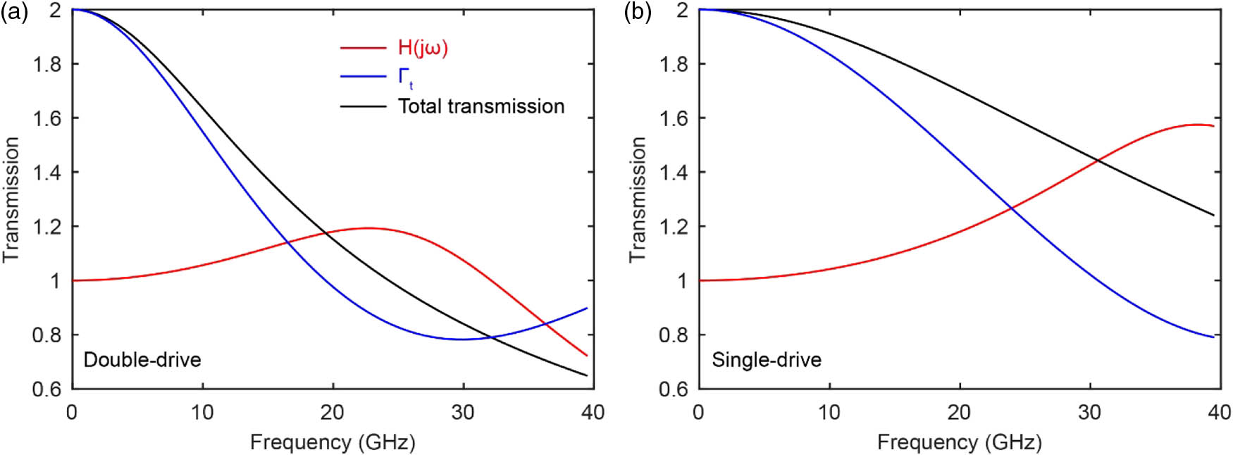
    Fig. 2. Frequency response of lumped modulators of (a) double-drive and (b) single-drive. Red, blue, and black lines represent the modulus of system transfer function H(jω), voltage transmission due to RF reflection Γt, and their product. Calculation uses VπLπ=1  V·cm.
    Large-signal characterization under 50 Ω standard characteristic impedance driver. Energy consumption relation with phase shifter length and doping concentration of (a) MZM and (b) MIM. The shown energy is obtained when Δϕ=0.1π. Bias voltages are chosen for each structural parameter so that the actual voltage on each PN junction is 0−−Vpp,eff. The lowest energy point (marked by “+”) in (a) is [L,N,E,Vin]=[0.350 mm,4.6×1017 cm−3,303.8 fJ/bit,6.12 V]; [L,N,E,Vin]=[0.375 mm,9.4×1017 cm−3,80.8 fJ/bit,1.95 V] in (b). Color represents log10(E) for better visual contrast. Eye diagrams of single-drive lumped modulators of (c)–(e) MZM and (f)–(h) MIM. The vertical axis is absolute value scale (not normalized). Doping concentration and phase shifter length for MZM and MIM are the optimal values in (a) and (b), respectively. Static working point: ϕ0=0.5π (biased at quadrature point). The driving “Vpp” specified in the figure is peak-to-peak voltage on each junction. Total input voltage is twice the value.
    Fig. 3. Large-signal characterization under 50 Ω standard characteristic impedance driver. Energy consumption relation with phase shifter length and doping concentration of (a) MZM and (b) MIM. The shown energy is obtained when Δϕ=0.1π. Bias voltages are chosen for each structural parameter so that the actual voltage on each PN junction is 0Vpp,eff. The lowest energy point (marked by “+”) in (a) is [L,N,E,Vin]=[0.350  mm,4.6×1017  cm3,303.8  fJ/bit,6.12  V]; [L,N,E,Vin]=[0.375  mm,9.4×1017  cm3,80.8  fJ/bit,1.95  V] in (b). Color represents log10(E) for better visual contrast. Eye diagrams of single-drive lumped modulators of (c)–(e) MZM and (f)–(h) MIM. The vertical axis is absolute value scale (not normalized). Doping concentration and phase shifter length for MZM and MIM are the optimal values in (a) and (b), respectively. Static working point: ϕ0=0.5π (biased at quadrature point). The driving “Vpp” specified in the figure is peak-to-peak voltage on each junction. Total input voltage is twice the value.
    Static IL under zero bias in the parameter space of interest. Modulation length is equal to the physical length of MZM and twice the physical length of MIM. The data used to obtain the coefficient is 1.12 dB/mm (N=1×1018 cm−3), not including propagation loss of the passive waveguide (typical value 0.2 dB/mm).
    Fig. 4. Static IL under zero bias in the parameter space of interest. Modulation length is equal to the physical length of MZM and twice the physical length of MIM. The data used to obtain the coefficient is 1.12  dB/mm (N=1×10¹⁸  cm3), not including propagation loss of the passive waveguide (typical value 0.2  dB/mm).
    Large-signal characterization under 10 Ω low-characteristic impedance driver. Energy consumption relation with phase shifter length and doping concentration of (a) MZM and (b) MIM. The shown energy is obtained when Δϕ=0.1π. Bias voltages are chosen for each structural parameter so that the effective voltage on each PN junction is 0−−Vpp,eff. The lowest energy point (marked by “+”) in (a) is [L,N,E,Vin]=[0.675 mm,6.4×1017 cm−3,66.9 fJ/bit,1.44 V]; [L,N,E,Vin]=[0.4625 mm,1.80×1018 cm−3,21.5 fJ/bit,0.774 V] in (b). (c)–(e) Eye diagrams of MIM modulators of the optimal parameters. Color represents log10(E) for better visual contrast. Static working point: ϕ0=0.5π (biased at quadrature point). The driving “Vpp” specified in the figure is peak-to-peak voltage on each junction. Total input voltage is twice the value.
    Fig. 5. Large-signal characterization under 10 Ω low-characteristic impedance driver. Energy consumption relation with phase shifter length and doping concentration of (a) MZM and (b) MIM. The shown energy is obtained when Δϕ=0.1π. Bias voltages are chosen for each structural parameter so that the effective voltage on each PN junction is 0Vpp,eff. The lowest energy point (marked by “+”) in (a) is [L,N,E,Vin]=[0.675  mm,6.4×1017  cm3,66.9  fJ/bit,1.44  V]; [L,N,E,Vin]=[0.4625  mm,1.80×1018  cm3,21.5  fJ/bit,0.774  V] in (b). (c)–(e) Eye diagrams of MIM modulators of the optimal parameters. Color represents log10(E) for better visual contrast. Static working point: ϕ0=0.5π (biased at quadrature point). The driving “Vpp” specified in the figure is peak-to-peak voltage on each junction. Total input voltage is twice the value.
    Xinbai Li, Fenghe Yang, Fang Zhong, Qingzhong Deng, Jurgen Michel, Zhiping Zhou. Single-drive high-speed lumped depletion-type modulators toward 10  fJ/bit energy consumption[J]. Photonics Research, 2017, 5(2): 134
    Download Citation