• Photonics Research
  • Vol. 1, Issue 2, 69 (2013)
E. Kasper1, M. Kittler2, M. Oehme1、*, and T. Arguirov2
Author Affiliations
  • 1University of Stuttgart, Institute of Semiconductor Engineering, Stuttgart, Germany
  • 2BTU Cottbus, Joint Lab IHP/BTU, Cottbus, Germany
  • show less
    DOI: 10.1364/PRJ.1.000069 Cite this Article Set citation alerts
    E. Kasper, M. Kittler, M. Oehme, T. Arguirov. Germanium tin: silicon photonics toward the mid-infrared [Invited][J]. Photonics Research, 2013, 1(2): 69 Copy Citation Text show less
    Si photonics scheme on an SOI wafer. Waveguides are from Si. Active devices are from Ge on Si.
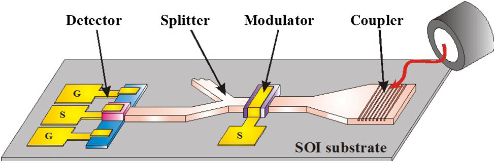
    Fig. 1. Si photonics scheme on an SOI wafer. Waveguides are from Si. Active devices are from Ge on Si.
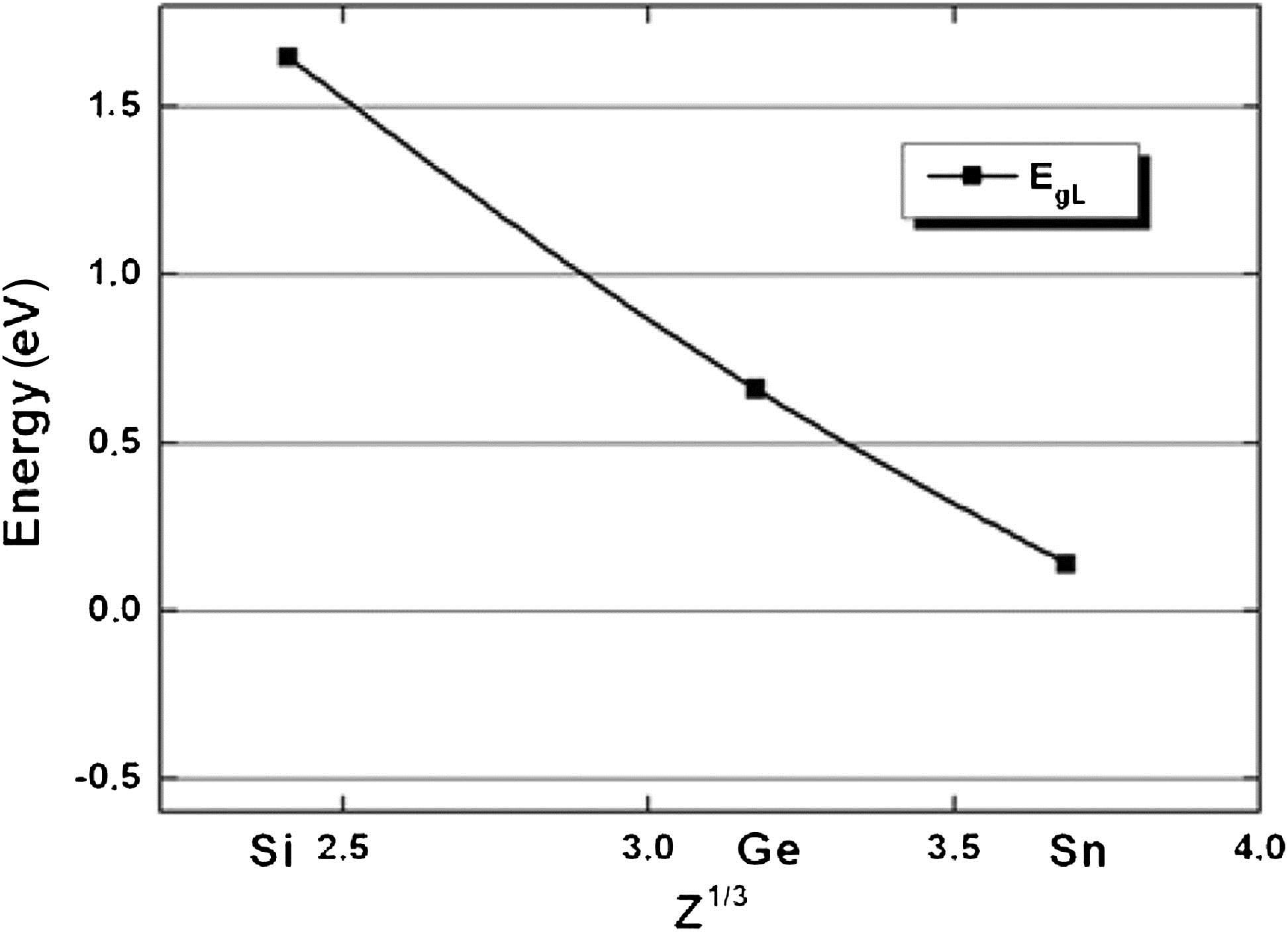
    Indirect bandgap EgL as function of atomic number (third root) Z1/3.
    Fig. 2. Indirect bandgap EgL as function of atomic number (third root) Z1/3.
    Energy difference ΔEg (L/Γ) between the indirect and direct gaps as a function of Z1/3. ΔEg=0 marks the crossover to a direct semiconductor.
    Fig. 3. Energy difference ΔEg (L/Γ) between the indirect and direct gaps as a function of Z1/3. ΔEg=0 marks the crossover to a direct semiconductor.
    Heteroepitaxial GeSn/Ge layers on Si and SOI substrates for photonic devices. The interfaces with misfit dislocation networks are marked.
    Fig. 4. Heteroepitaxial GeSn/Ge layers on Si and SOI substrates for photonic devices. The interfaces with misfit dislocation networks are marked.
    Equilibrium phase diagram of Ge–Sn. Shown is the Ge rich side up to 15% Sn.
    Fig. 5. Equilibrium phase diagram of Ge–Sn. Shown is the Ge rich side up to 15% Sn.
    Critical epitaxial thickness h1 as function of the Sn fraction x in GeSn/Si (relaxed GeSn) and GeSn/Ge (compressive strained GeSn). Inset shows data from Bratland et al. [35].
    Fig. 6. Critical epitaxial thickness h1 as function of the Sn fraction x in GeSn/Si (relaxed GeSn) and GeSn/Ge (compressive strained GeSn). Inset shows data from Bratland et al. [35].
    Extraction of direct bandgap for different Sn contents of GeSn from responsivity Ropt measurements.
    Fig. 7. Extraction of direct bandgap for different Sn contents of GeSn from responsivity Ropt measurements.
    Decrease of ΔEg of the direct bandgap with GeSn of increasing Sn content. Compared are experiment values with theory.
    Fig. 8. Decrease of ΔEg of the direct bandgap with GeSn of increasing Sn content. Compared are experiment values with theory.
    EL spectra of compressively strained GeSn LEDs on Ge VS with different Sn content. The intensity maximum was normalized to 100% to make clear the infrared shift (lower energy) obtained with few percent Sn incorporation.
    Fig. 9. EL spectra of compressively strained GeSn LEDs on Ge VS with different Sn content. The intensity maximum was normalized to 100% to make clear the infrared shift (lower energy) obtained with few percent Sn incorporation.
    Ellipsometry of epitaxial GeSn layers up to 20% Sn content. Shown are the refractive index n and the absorption constant k as functions of the wavelength.
    Fig. 10. Ellipsometry of epitaxial GeSn layers up to 20% Sn content. Shown are the refractive index n and the absorption constant k as functions of the wavelength.
    Maximum position (wavelength) of the refractive index as a function of the lattice constants of SiGe and GeSn.
    Fig. 11. Maximum position (wavelength) of the refractive index as a function of the lattice constants of SiGe and GeSn.
    In situ reflection measurements of epitaxial GeSn on Si at wavelengths of 470 and 950 nm.
    Fig. 12. In situ reflection measurements of epitaxial GeSn on Si at wavelengths of 470 and 950 nm.
    Raman scattering of GeSn on Si. Shown is the region around the Ge–Sn phonon peak.
    Fig. 13. Raman scattering of GeSn on Si. Shown is the region around the Ge–Sn phonon peak.
    ElementSiGeα-Sn
    Z143250
    EgL (eV)1.12 (X), 1.65 (L)0.664 (L)0.14 (L)
    ΔEg (eV)2.10.1360.55
    a0 (nm)0.54310.56460.6489
    Table 1. Summary of the Properties EgaΔEb, and a0c for the Elements Si, Ge, and α-Sn
    E. Kasper, M. Kittler, M. Oehme, T. Arguirov. Germanium tin: silicon photonics toward the mid-infrared [Invited][J]. Photonics Research, 2013, 1(2): 69
    Download Citation