E. Kasper, M. Kittler, M. Oehme, T. Arguirov, "Germanium tin: silicon photonics toward the mid-infrared [Invited]," Photonics Res. 1, 69 (2013)
Copy Citation Text
Germanium tin (GeSn) is a group IV semiconductor with a direct band-to-band transition below 0.8 eV. Nonequilibrium GeSn alloys up to 20% Sn content were realized with low temperature (160°C) molecular beam epitaxy. Photodetectors and light emitting diodes (LEDs) were realized from in situ doped pin junctions in GeSn on Ge virtual substrates. The detection wavelength for infrared radiation was extended to 2 μm with clear potential for further extension into the mid-infrared. GeSn LEDs with Sn content of up to 4% exhibit light emission from the direct band transition, although GeSn with low Sn content is an indirect semiconductor. The photon emission energies span the region between 0.81 and 0.65 eV. Optical characterization techniques such as ellipsometry, in situ reflectometry, and Raman spectroscopy were used to monitor the Sn incorporation in GeSn epitaxy.
Silicon photonics has seen a strong increase in research activity, technology platforms, and commercial startups from silicon waveguides on silicon-on-insulator (SOI) substrates. These waveguides are the leading ones in terms of high refractive index contrast, small footprint, and integration potential with silicon (Si)-based microelectronics [1]. Intrinsic Si waveguides are transparent from the near-infrared (NIR) to the mid-infrared (MIR), from 2 to 5 μm wavelengths, and partly also in the far-infrared (FIR), from above 5 μm, depending on the oxygen and hydrogen content. A fundamental limit is above the 20 μm wavelength when phonon absorption sets in. The lower waveguide cutoff is determined by the indirect bandgap (at room temperature, the bandgap ), and phonon-assisted () absorption starts at 1.06 eV, corresponding to about a 1.2 μm wavelength.
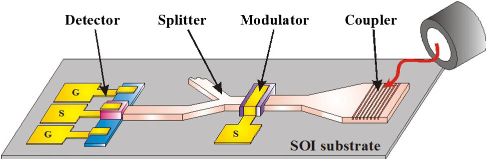
Above the cutoff wavelength of 1.2 μm, the transparent Si waveguide transports, splits, and combines optical signals and influences signals through phase difference effects (the Mach–Zehnder interferometer principle). Active devices that generate, detect, and convert optical signals into electrical ones are not available in the transparency regime because these require matter–light interactions. Recent technical solutions changed rapidly from hybrid integration to monolithic integration (Fig. 1) of germanium (Ge) active devices. Despite a rather large lattice mismatch (4.2%) for hard materials, Ge-on-Si devices obtained in NIR high-speed operation (50 GHz) [2] good quantum efficiency [3], a strong quantum confined Stark effect [4], and the Franz–Keldysh effect [5] for absorption modulators and, recently, as strong highlights optically stimulated [6] and electrically stimulated [7] laser radiation are demonstrated. The upper cutoff wavelength is given by the Ge direct transition bandgap of 0.8 eV. (Ge is an indirect semiconductor with a 0.664 eV bandgap at room temperature, but in small dimension devices the indirect transition is too weak to be utilized. Larger indirect than direct luminescence in bulk Ge turned out to be caused by self-absorption effects [8].) With slight tensile strain (0.25%) the upper cutoff wavelength [6] is about 1.6 μm because tensile strain reduces the bandgap. Tensile strain in Ge device structures is obtained from thermal expansion mismatch between the Si substrate and the Ge film after annealing [9]. Further extension of the spectral range of Si-based photonics from Ge-on-Si—this is from 1.2 to 1.6 μm—into the MIR range (2–5 μm) is highly welcome for a couple of reasons (bandwidth, medical, and biological applications), which are summarized in a recent presentation [10].
Figure 1.Si photonics scheme on an SOI wafer. Waveguides are from Si. Active devices are from Ge on Si.
A straightforward extension of the spectral range is given by a small bandgap semiconductor. A smaller bandgap strengthens the tendency to direct semiconductors, which nurtures the hope for efficient light emission and lasing in the MIR.
Sign up for Photonics Research TOC. Get the latest issue of Photonics Research delivered right to you!Sign up now
In the following sections we present first the expectations based on the only group IV semiconductor [germanium tin (GeSn)] with low bandgap. Then the material and device challenges of GeSn-on-Si are presented, and the recent status of device work on photoconduction, diode detectors, and light emitting diodes (LEDs) is used as a measure of progress. The basic optical characterization method on epitaxial films of GeSn-on-Si led to predictions of future routes to close the gap between theoretical expectations and nonequilibrium material preparation.
2. EXPECTATIONS OF A DIRECT GROUP IV SEMICONDUCTOR: GeSn
The group IV element series C, Si, Ge, and Sn exhibit semiconducting modifications with diamond lattice structures. Within the same lattice structure, systematic trends with increasing atomic number allow prediction of alloy properties good enough for projecting expectations. For GeSn-on-Si we concentrate on the bandgap , on the energy difference between direct and indirect transitions, and on the lattice mismatch between Si–Ge–Sn.
Many properties (see Table 1) may be drawn as near-linear functions [11] of the third root of (), whereas a presentation of property versus alloy composition requires strong parabolic deviation if electronegativity and atomic size of the alloy partners differ strongly.
Element
Si
Ge
α-Sn
Z
14
32
50
EgL (eV)
1.12 (X), 1.65 (L)
0.664 (L)
0.14 (L)
ΔEg (eV)
2.1
0.136
−0.55
a0 (nm)
0.5431
0.5646
0.6489
Table 1. Summary of the Properties ab, and c for the Elements Si, Ge, and -Sn
With increasing atomic number , the transition energies from the conduction band to the valence band shrink (Table 1). Figure 2 shows the transition energy , which from SiGe (Ge content 0.85) on is the lowest lying indirect transition, and which determines around Ge the indirect character of the semiconductor alloys SiGe (from 85% Ge on) and GeSn (up to 10% Sn). The corresponding indirect bandgap cutoff wavelength increases to more than 2.5 μm.
Figure 2.Indirect bandgap as function of atomic number (third root) .
Expectations are to increase the spectral window for Si-based photonics to the MIR with GeSn of rather low Sn content.
B. Direct Semiconductor from Group IV Material
The usual group IV semiconductors are indirect ones, which means the transition from the lowest lying conduction band state to the valence band needs the participation of phonons to fulfill the momentum condition. The corresponding strong reduction in the radiative transition rate makes it difficult to get efficient LEDs or lasers from indirect semiconductors.
The semiconducting modification of tin (-Sn) is a zero bandgap semiconductor with a direct bandgap of . Why is zero bandgap material not a metal, and what means a direct gap of (Table 1)? The conduction band and valence band overlap only at certain wavevectors (at zero momentum the overlap is 0.41 eV), whereas at other wavevector regimes there is a gap between them, which satisfies the requirements to call this interesting material a semiconductor.
A crossover between direct transitions and indirect transitions in GeSn is expected at rather low Sn content when we plot the energy difference () between the indirect valley and the direct point as a function of (Fig. 3). More accurate models consider the deviation from linear interpolation by a parabolic dependence: where is the corresponding bandgap for Ge, is the bandgap difference between Ge and Sn [do not confuse with () as mentioned before, which measures the bandgap difference between direct and indirect transitions in the same material], is the molar Sn concentration, and is the parabolicity constant.
Figure 3.Energy difference () between the indirect and direct gaps as a function of . marks the crossover to a direct semiconductor.
The crossover point where the semiconductor GeSn may be expected to get direct is around a Sn content of 10%. The uncertainty is caused by combining experimental room temperature values for Ge with model calculation for Sn and uncertain values of the parabolicity constant . The bandgap energy and transition wavelength at the crossover point are expected to be around 0.5 eV and 2.5 μm, respectively.
The expectations are that with GeSn, efficient LEDs from the 2 μm wavelength on and MIR lasers from 2.5 μm on may be realized if the material quality is sufficient to suppress competing nonradiative recombination.
C. Layer Structures for Photonic Devices
The lattice mismatch between -Sn (semiconducting diamond lattice cell, ) and Si () is rather high. Even for Ge rich GeSn alloys the lattice mismatch is more than 4.3%.
The mismatch between Ge and -Sn amounts to 14.7%. The lattice constant of GeSn is roughly described by a linear law [12] so that the crossover (around 10% GeSn) takes place at a lattice mismatch of 1.5% between GeSn and Ge.
The light emitting structure is usually placed on a so-called “virtual substrate” (VS), which [11] consists of the rigid Si substrate and a buffer layer on top. The buffer layer serves as accommodation to a different lattice cell. Typical buffer layer materials for GeSn films are relaxed Ge or relaxed GeSn itself. Figure 4 shows, from left to right, direct growth of GeSn on Si; (b) growth of GeSn on Ge VS (relaxed Ge buffer on Si). The strain status is either compressive or relaxed depending on thickness and growth/annealing temperatures; (c) Ge on GeSn VS. Tensile strain for Ge is obtained if the thickness is thin, below the critical thickness for misfit dislocation formation at the VS/Ge interface. Selective epitaxy of GeSn along a Ge film gives compressive strain for the Ge as preferred for -MOSFETs. This configuration is not treated here.
Figure 4.Heteroepitaxial GeSn/Ge layers on Si and SOI substrates for photonic devices. The interfaces with misfit dislocation networks are marked.
The lattice mismatch between the different heterostructures results in misfit dislocation networks at the Si substrate film interface and another one between relaxed GeSn and Ge VS.
3. MATERIAL AND DEVICE CHALLENGES
Already in the 1980s and 1990s, several groups were investigating the fabrication of -Sn [13–16] or GeSn alloys [17–22]. However several challenges for the single crystalline growth of GeSn alloys were found. Only the diamond structure of -Sn is semiconducting. This phase is only stable at temperatures below 13.2°C. At higher temperatures, -Sn transforms to the metallic phase -Sn. For fabrication of heterostructures the huge lattice mismatch between -Sn () and Ge () of 14.7% has to be overcome. In contrast to the SiGe alloy, which is completely miscible, the solid solubility of Sn in Ge is extremely low with 1% (Fig. 5). Furthermore, at growth temperatures higher than 140°C the surface segregation of Sn is extremely high. All investigations from the 1980s and 1990s showed that growth conditions far away from the thermodynamic equilibrium have a chance to produce monocrystalline GeSn alloys. As an example of the refined growth methods developed in those early days, we mention the synthesis of Sn/Ge/Si superlattices [21] by temperature modulation molecular beam epitaxy (MBE) and the epitaxial growth of high Sn content alloys [19] on group III/V substrates (InSb).
Figure 5.Equilibrium phase diagram of Ge–Sn. Shown is the Ge rich side up to 15% Sn.
From the phase diagram one sees immediately the problems of equilibrium growth of GeSn. Sn has a low melting point (about 500 K). That means at growth temperatures above 500 K a two-phase mixture is created: solid Ge (diamond lattice with very small Sn amount, below 1%) and liquid Sn. Below 500 K a two-phase solid mixture is created, again with diamond lattice Ge (small Sn amount) and body centered cubic (metallic) Sn. A single phase is created only at the end points, either with a very small Sn amount () or with a very high Sn amount ().
GeSn solid solutions with a few percent Sn content can be grown only under nonequilibrium conditions. Groups in Japan (Takeuchi and co-workers [23,24]), the U.S. (Cook and co-workers [25–27]), and in Mexico (de Guevera et al.[28]) developed specific MBE, chemical vapor deposition, and sputtering techniques, respectively, and they restarted GeSn work with an emphasis on optical properties and photonic device applications.
We have to suppress phase separation. Separation takes place either on the surface (surface segregation) or in the volume (precipitation). Kinetic suppression of phase separation requires very low growth temperatures, which itself causes difficulties with point defect concentrations and amorphization tendency. A high lattice mismatch (the Sn lattice is about 15% larger than that of Ge) is given between Sn and Ge [29]. For Ge rich GeSn solutions the lattice mismatch is within a regime known from SiGe/Si epitaxy.
A. Surface Segregation
Surface segregation is a widely known phenomenon in epitaxy. Rather well-investigated systems are Sb/Si [30] and B/Si [31], from which we can draw a general picture. The driving force is the energy gain if a matrix adatom changes its position with an underlying (subsurface atom) dopant atom. In our case the matrix atom is Ge and the dopant atom is Sn (in this context we call the minority atom species a dopant without considering the electrical effects). For simplicity, let us consider a linear segregation model, which implicitly means a constant surface energy independent from surface coverage and is an acceptable assumption up to 0.1 monolayer coverage. In this case, the surface adatom concentration is linked linearly with the bulk concentration of the dopant:
The linear coefficient is the segregation length, the value of which is determined at low epitaxy temperatures for kinetic reasons. The kinetic branch has to be considered for GeSn because of the necessary nonequilibrium growth conditions. The segregation length determines the highest obtainable concentration and the concentration slope after switch on/off of the Sn source. The segregating Sn on the surface may show a phenomenon not known from the other group IV epitaxy systems. Above the Sn on the surface melts; the melting point is probably somewhat above the bulk melting point of 200°C. The kinetic branch of the segregation length is strongly dependent on temperature (segregation length decreases with lower temperature) and dependent on growth rate (segregation length decreases with higher growth rate). Both results can be understood on the basis of the simple model. The exchange rate is faster at higher temperatures, and the time slot is smaller for higher growth rates. Only unsystematic data on segregation of Sn on Ge are available. We mention, therefore, as an example a better investigated system, Ge/Si [30].
B. Precipitations
In a two-phase system, the phase separation in the bulk happens via nucleation and extension of precipitations. A supersaturated GeSn solution would then break up into a Ge:Sn matrix with Sn:Ge precipitations. Precipitation has to overcome energetic barriers (nucleation of a strained Sn:Ge nucleus) and kinetic barriers (diffusion of Sn atoms to the nucleus) so that, during growth, dominance of surface segregation may be assumed. High enough temperatures during device processing could, however, promote precipitations. Device fabrication demonstrated that the supersaturated solution stays stable up to 600°C annealing, at least for small Sn contents ().
C. Low Temperature Growth
From the previous sections it becomes clear that growth of supersaturated GeSn requests a high growth rate and/or low growth temperatures. However, low growth temperatures tend to favor excess point defect levels or even a breakdown of crystalline growth into an amorphous one. We present here a general model of the defect generation that narrows the epitaxy window for device structures and we propose an in situ method to follow the phenomenon. In the regular epitaxy temperature regime the nearly perfect lattice arrangement is repeated with each monolayer deposition. This requires that a huge amount [ on a Si (100) surface] of adatoms, which at random positions, will find their correct lattice position within a short time frame (typically 1 s for a growth rate). At very low growth temperatures a certain percentage of adatoms will not find the lattice positions, creating point defects (vacancies, interstitials). The next layers will be disturbed above the underlying defect and add additional defects. In this model the later layers will have more defects than the first ones. This model simplifies because defects in semiconductor bulk are rather mobile, which leads to defect annihilation by interstitial–vacancy reaction or defect surface reaction. The general description is real as demonstrated by a critical thickness of epitaxial growth (). This critical thickness may not be confused with the critical thickness for misfit dislocation generation in strained layers. The concept of critical thickness of epitaxy [32] is related to low temperature epitaxy, and it can be considered as proof for defect accumulation with progressing low temperature growth. The defect accumulation was also electrically directly proofed in Esaki diode junction operation [33]. An elegant in situ measurement of the critical epitaxial thickness is based on interferometric reflectometry [34] utilizing the refractive index changes at the crystalline/amorphous transition.
The phenomenon of decreasing quality with increasing thickness during low temperature epitaxy is called “epitaxial breakdown.” For GeSn growth the epitaxial breakdown was investigated in detail in [35].
Several parameters, such as residual gas content in the epitaxy chamber (already small amounts of contamination—submonolayers—promote epitaxial breakdown because the contamination is not desorbing at the low temperatures), growth rate, true wafer temperature (at very low growth temperatures only the ambient temperature may be controlled), and nonthermal energy supply (e.g., ions or electrons), may influence the results. In Fig. 6 we compare our results for epitaxial breakdown with [35].
Figure 6.Critical epitaxial thickness as function of the Sn fraction in GeSn/Si (relaxed GeSn) and GeSn/Ge (compressive strained GeSn). Inset shows data from Bratland et al. [35].
Strong absorption connected with direct transition is a very stable property of semiconductors that does not depend much on impurities and defects. For new epitaxial materials the indirect measurement of absorption from photoresponsivity is in common use. For low epitaxial thicknesses (low means thinner than the penetration depth of light in that material) and a limited spectral range above the bandgap cutoff the responsivity is proportional to the absorption coefficient . The absorption coefficient of a direct transition depends on the photon energy as.
A plot of versus phonon energy allows us to immediately extract the direct band edge . Absorption below the direct bandgap energy is influenced by the lower lying indirect transitions ( and valleys) and by excitonic effects [36]. The constant depends on the common density of states, which is proportional to the square root of the effective mass.
Photodetection in semiconductors is mainly based on the internal photoeffect in the depletion region of a ‒ junction. Absorbed photons generate electron–hole pairs, which are separated by the electric field and detected as photocurrent. These photodetectors by diode structures exhibit good performance concerning spectral range, quantum efficiency, low noise and high speed. But they need rather high crystalline quality and a ‒ junction technology that is not self-evident in nonequilibrium alloy films. Less demanding on quality and device technology are photoconductive detectors that rely on conductivity modulation by the additional carriers generated from absorption. Both types of photodetectors are realized in GeSn. A good example of the photoconductive detector is given by Gassenq et al.[37]. Photodiodes are realized by several groups [38] with low Sn contents. Variation of Sn content and resulting changes in the bandgap energies are shown in Fig. 7.
Figure 7.Extraction of direct bandgap for different Sn contents of GeSn from responsivity measurements.
One sees immediately from Fig. 7 that the linear extrapolation of versus (, optional responsivity; photon energy) delivers direct bandgaps, which extend to lower energies with increasing Sn content. The slope of the linear extrapolation decreases with Sn content, which can be taken as a hint of smaller effective masses in GeSn alloys compared to Ge. Direct bandgap measurements with different methods [39] are summarized in Fig. 8 and compared with model calculations of D’Costa et al.[40] and Alberi et al.[41].
Figure 8.Decrease of of the direct bandgap with GeSn of increasing Sn content. Compared are experiment values with theory.
The given data confirm undoubtedly the spectral range extension of GeSn devices on Ge on Si into MIR. A wavelength of 2 μm is obtained with about a mere 5% Sn content. A comparison with the model of Alberi et al. gives a rather good agreement between theory and experiments. But the theory is for strain relaxed material and the experimental evidence is for compressive strained GeSn. The layer structures of our group are fully strained after epitaxy, but device processing may yield partial relaxation, which is not as easily measurable in devices as on flat layer structures. Relaxation of compressive strain pushes the bandgap further into the infrared, which is documented by photoreflectance measurements in [42].
5. ELECTROLUMINESCENCE DEVICES
Electroluminescence (EL) devices that are based on band-to-band transitions are very sensitive to material quality and device processing issues because defects open competing nonradiative recombination paths. The main sources of concern about epitaxial material quality stem from dislocations and point defects, basic processing issues that are given by the annealing stability of metastable low temperature grown GeSn and by technical questions (doping, etching, and passivation of GeSn).
The open material and process issues resulted in only few realizations of light emitting devices [43]. The best results were obtained with GeSn diodes on Ge VS. But these devices are compressively strained with a bandgap difference () not much different from Ge. Sn content decreases the difference, but compressive strain increases it.
The EL emission spectra of such compressively strained GeSn are shown in Fig. 9. The integral intensity of the light is same or lower than in Ge diodes; for easier comparison of energy position and line shape we have normalized the peak intensity to 100%.
Figure 9.EL spectra of compressively strained GeSn LEDs on Ge VS with different Sn content. The intensity maximum was normalized to 100% to make clear the infrared shift (lower energy) obtained with few percent Sn incorporation.
Clearly seen is the redshift of the peak positions in agreement with earlier photoluminescence (PL) and absorption measurements. The line shape is broadened basically by strain splitting of the heavy hole (hh) and light hole (lh) states of the valence band. In compressive strained material the hh transition is lower in energy, and it is the dominating one because the intensity of lh transitions is about a factor of 4 smaller because of lower effective mass and correspondingly lower effective density of states.
6. OPTICAL CHARACTERIZATION
Nondestructive optical techniques are demanded for characterization of thin (submicrometer) epitaxial layer structures and for control of device processing. We address here ellipsometry, in situ reflection, and Raman spectroscopy.
A. Ellipsometry
Ellipsometry delivers rich information about thickness, refractive index , and absorption constant (extinction coefficient) . The absorption coefficient is related to by
We have measured and of thin GeSn layers on Si by fitting the experimental data to a seven-oscillator model (Fig. 10). The Sn incorporation shifts all signatures toward a higher wavelength that is similar to the bandgap. The highest optical influence stems from the conduction subband like in Si and Ge. The corresponding maximum in refractive index is a good indication of the chemical composition.
Figure 10.Ellipsometry of epitaxial GeSn layers up to 20% Sn content. Shown are the refractive index and the absorption constant as functions of the wavelength.
Figure 11 shows the wavelength position of this maximum for different lattice constants. Given as abscissa is not the lattice constant itself but the lattice mismatch to Si. Lattice mismatch is calculated from a linear interpolation (Vegard’s law). This presentation allows us to display SiGe data and GeSn data on the same plot.
Figure 11.Maximum position (wavelength) of the refractive index as a function of the lattice constants of SiGe and GeSn.
Reflection measures only amplitudes, not phase, of the reflected beam. It does not give the same full information as ellipsometry, but the ease of use makes it very suitable to in situ measurements in epitaxy equipment. Figure 12 shows in situ reflectivity measurements for MBE-grown GeSn layers on Si. For a semitransparent measurement wavelength (950 nm), a damped oscillation of reflectivity is observed from whose amplitude and thickness difference the refractive index can be calculated. For a strong absorbing wavelength (470 nm), a damped approaching to the bulk value is observed. Changes in this value are related to surface smoothness.
Figure 12.In situ reflection measurements of epitaxial GeSn on Si at wavelengths of 470 and 950 nm.
Only a small amount of the light reflected from a film is shifted in energy by the Raman scattering from optical phonons. In alloys like GeSn one expects, in a simple model, Raman shifts from Ge–Ge, Ge–Sn, and Sn–Sn phonon vibrations but also localized modes may be seen. Figure 13 shows Raman spectra (intensity versus wave number difference from the probe laser, here a 633 nm laser wavelength). The strong peak below belongs to the dominating Ge–Ge phonons, the peak at around is assigned to the Ge–Sn vibration, and the vibration around is tentatively called Sn-like. The exact wave number position of the peaks reflects the influence of chemical composition and strain.
Figure 13.Raman scattering of GeSn on Si. Shown is the region around the Ge–Sn phonon peak.
Mankind has known the metal tin for more than 3000 years; it was mainly used for alloying with other metals, especially copper. In medieval times, pure tin was used for manufacture of precious drinking cups. The material quality of the cups degraded with time, which was called “tin pest” in analogy to severe illness, the causes of which were also not understood at that time. Now we know the cause of tin pest: a switch between two modifications of tin, the well-known metal (now called -Sn) and a semiconducting modification (-Sn), which is stable below 13.2°C.
During the past three decades, -Sn has been investigated for basic physics reasons because it is a zero bandgap semiconductor. The alloy with the next group IV semiconductor, GeSn, turned out to be stable at equilibrium with only very small content of the partner material.
The next step was devoted to synthesized GeSn alloys with larger Sn content as given under equilibrium conditions. Low temperature epitaxy of GeSn has overcome Sn content limitations at least up to 20% with thin layers below epitaxial breakdown. Only in the past few years has device work started with technologies similar to Ge-on-Si devices. All these device investigations proved that a few percent Sn incorporation shifted the cutoff wavelength into the MIR. A continuation of this trend toward higher Sn content and larger cutoff wavelengths is predicted.
Different is the situation with light emitting devices. However, the shift to lower emission energies was confirmed, even with compressive strained layers. However, the crossover to a direct bandgap semiconductor with orders of magnitude higher emission intensity is still missing.
Substantial improvements in epitaxial material quality and in low temperature device processing are required to demonstrate lasing from a direct group IV semiconductor. Future routes to overcome the limits are reduction of the point defect densities in low temperature epitaxy and processing of strain relaxed structures. Careful annealing procedures without promoting Sn precipitation are of key importance to obtain these goals.
References
[1] E. Kasper. Prospects and challenges of silicon/germanium on-chip optoelectronics. Front. Optoelectron. China, 3, 143-152(2009).
[28] H. P. L. de Guevara, H. Navarro-Contreras, M. A. Vidal. Growth and characterization of Ge1−xSnx alloys grown by magnetron sputter deposition. Superficies y Vacio, 16, 22-24(2003).
[29] J. Xie, J. Tolle, V. R. D’Costa, C. Weng, A. V. G. Chizmeshya, J. Menendez, J. Kouvetakis. Molecular approaches to p-and n-nanoscale doping of . Solid State Electron., 53, 816-823(2009).
[30] H. Jorke, E. Kasper, K. Lyutovich. Properties of Strained and Relaxed SiGe, 287(2000).