• Infrared and Laser Engineering
  • Vol. 51, Issue 1, 20210976 (2022)
Yuqing Guan1、2, Yunxia Fu1、2, Wenzhe Zou1、2, Zhangning Xie3, and Lihua Lei1、2、*
Author Affiliations
  • 1Shanghai Institute of Measurement and Testing Technology, Shanghai 201203, China
  • 2Shanghai Key Laboratory of Online Test and Control Technology, Shanghai 2012032, China
  • 3School of Physical Science and Engineering, Tongji University, Shanghai 200082, China
  • show less
    DOI: 10.3788/IRLA20210976 Cite this Article
    Yuqing Guan, Yunxia Fu, Wenzhe Zou, Zhangning Xie, Lihua Lei. A characterization method of thin film parameters based on adaptive differential evolution algorithm (Invited)[J]. Infrared and Laser Engineering, 2022, 51(1): 20210976 Copy Citation Text show less
    Optical path diagram of system construction
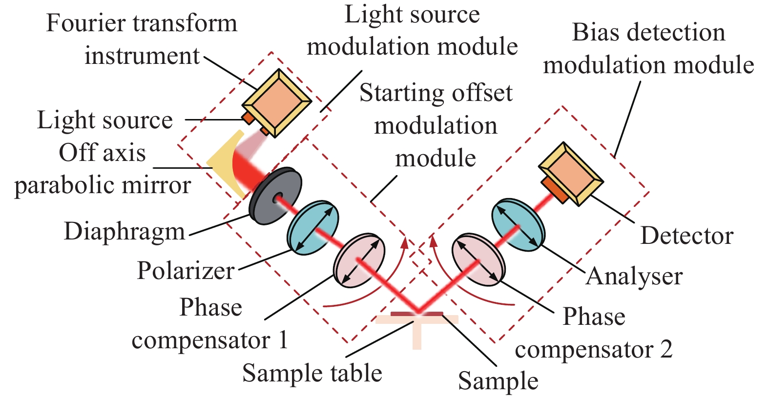
    Fig. 1. Optical path diagram of system construction
    Flow chart of adaptive differential evolution algorithm
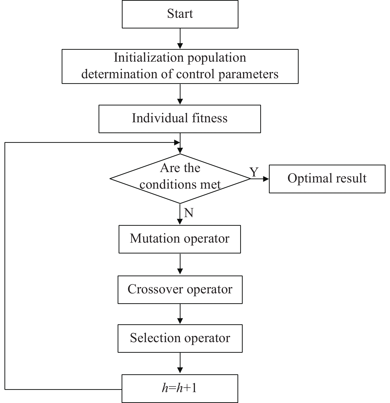
    Fig. 2. Flow chart of adaptive differential evolution algorithm
    Iterative curve of 104.2 nm SiO2/Si standard sample
    Fig. 3. Iterative curve of 104.2 nm SiO2/Si standard sample
    Iterative curve of 398.4 nm SiO2/Si standard sample
    Fig. 4. Iterative curve of 398.4 nm SiO2/Si standard sample
    Mueller spectrum of 104.2 nm SiO2/Si film thick sample
    Fig. 5. Mueller spectrum of 104.2 nm SiO2/Si film thick sample
    Mueller spectrum of 398.4 nm SiO2/Si film thick sample
    Fig. 6. Mueller spectrum of 398.4 nm SiO2/Si film thick sample
    Index of refractive and extinction coefficient of 104.2 nm standard sample
    Fig. 7. Index of refractive and extinction coefficient of 104.2 nm standard sample
    Index of refractive and extinction coefficient of 398.4 nm standard sample
    Fig. 8. Index of refractive and extinction coefficient of 398.4 nm standard sample
    Iterative curve of 104.2 nm SiO2/Si standard sample
    Fig. 9. Iterative curve of 104.2 nm SiO2/Si standard sample
    Iterative curve of 398.4 nm SiO2/Si standard sample
    Fig. 10. Iterative curve of 398.4 nm SiO2/Si standard sample
    Measurement of ellipsometry parameters of 104.2 nm SiO2/Si standard sample
    Fig. 11. Measurement of ellipsometry parameters of 104.2 nm SiO2/Si standard sample
    Measurement of ellipsometry parameters of 398.4 nm SiO2/Si standard sample
    Fig. 12. Measurement of ellipsometry parameters of 398.4 nm SiO2/Si standard sample
    ElementParameterCalibration value/(º)
    Polarizer POrientation AS45
    Waveplate C1Initial orientation c10
    Waveplate C1Retardation Δ190
    Waveplate C2Initial orientation c20
    Waveplate C2Retardation Δ290
    Analyzer AOrientation PS−45
    Table 1. System component parameter values
    Mueller elementFitting error
    m120.386
    m210.386
    m330.258
    m340.232
    m430.374
    m440.392
    Table 2. MSE of 104.2 nm sample
    Mueller elementFitting error
    m120.412
    m210.412
    m330.365
    m340.409
    m430.384
    m440.422
    Table 3. MSE of 398.4 nm sample
    Film thickness/nmCalculated film thickness/nmRelative error
    104.2±0.4103.8±0.60.38%
    398.4±0.4397.8±0.60.15%
    Table 4. Calculated value of sample thickness
    Film thickness /nm AlgorithmNumber of iterationsIteration time/sCalculated film thickness/nmRelative error
    104.2SADE681.22103.8±0.60.38%
    LM541.13104.6±0.60.78%
    398.4SADE821.47397.8±0.60.15%
    LM561.21401.1±0.60.82%
    Table 5. Comparison of experimental results
    Film thickness/nmCalculated film thickness/nmRelative error
    104.2±0.4104.1±0.60.09%
    398.4±0.4398.2±0.60.05%
    Table 6. Calculated value of sample thickness
    Yuqing Guan, Yunxia Fu, Wenzhe Zou, Zhangning Xie, Lihua Lei. A characterization method of thin film parameters based on adaptive differential evolution algorithm (Invited)[J]. Infrared and Laser Engineering, 2022, 51(1): 20210976
    Download Citation