• Photonics Research
  • Vol. 11, Issue 11, 1870 (2023)
Yunqing Jiang1、2、†, Xiaoqiang Zhang1、2、†,*, Houyi Cheng1、2、†, Huan Liu3, Yong Xu1、2、6, Anting Wang4, Cong Wang1, Stéphane Mangin5, and Weisheng Zhao1、2
Author Affiliations
  • 1School of Integrated Circuit Science and Engineering, Hefei Innovation Research Institute, Beihang University, Beijing 100191, China
  • 2Anhui High Reliability Chips Engineering Laboratory, Hefei 230013, China
  • 3School of Energy and Power Engineering, Beihang University, Beijing 100191, China
  • 4Department of Optics and Optical Engineering, University of Science and Technology of China, Hefei 230026, China
  • 5Institut Jean Lamour, UMR CNRS 7198, Universite de Lorraine, Nancy 54011, France
  • 6e-mail: yongxu@buaa.edu.cn
  • show less
    DOI: 10.1364/PRJ.497939 Cite this Article Set citation alerts
    Yunqing Jiang, Xiaoqiang Zhang, Houyi Cheng, Huan Liu, Yong Xu, Anting Wang, Cong Wang, Stéphane Mangin, Weisheng Zhao. Resonance cavity-enhanced all-optical switching in a GdCo alloy absorber[J]. Photonics Research, 2023, 11(11): 1870 Copy Citation Text show less
    Schematic of the AOS in (a) FTF and (b) CE-FTF. The FTF is composed of Pt/GdCo/Pt/Ta. Equivalent transmission line mode of (c) FTF and (d) CE-FTF. In the equivalent circuit model, the FTF is equivalent to a load with a conductivity of σFTF, and the added Au layer induces a short circuit. Insets show the magnetic domain state, where the black contrast corresponds to the initial magnetization, and the white contrast corresponds to a magnetization reversal.
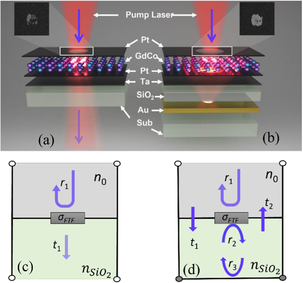
    Fig. 1. Schematic of the AOS in (a) FTF and (b) CE-FTF. The FTF is composed of Pt/GdCo/Pt/Ta. Equivalent transmission line mode of (c) FTF and (d) CE-FTF. In the equivalent circuit model, the FTF is equivalent to a load with a conductivity of σFTF, and the added Au layer induces a short circuit. Insets show the magnetic domain state, where the black contrast corresponds to the initial magnetization, and the white contrast corresponds to a magnetization reversal.
    (a) Conductivity of the FTF as a function of the thickness of the GdCo alloy, and the thicknesses of Pt and Ta layers are 2 and 3 nm, respectively. (b) Optical absorption of each layer and the total absorption of the FTF under different thicknesses of the GdCo alloy. (c) Phase diagram of the optical absorption of the GdCo alloy as a function of its thickness tGdCo and the thickness of the inserted dielectric layer d. (d) Absorption of each layer of the CE-FTF under different thicknesses of the inserted dielectric layer d with the thickness of tGdCo=8 nm.
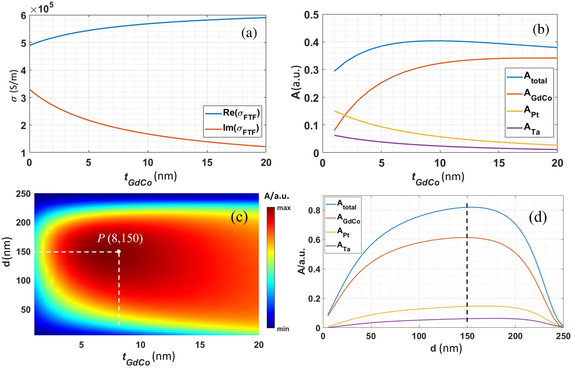
    Fig. 2. (a) Conductivity of the FTF as a function of the thickness of the GdCo alloy, and the thicknesses of Pt and Ta layers are 2 and 3 nm, respectively. (b) Optical absorption of each layer and the total absorption of the FTF under different thicknesses of the GdCo alloy. (c) Phase diagram of the optical absorption of the GdCo alloy as a function of its thickness tGdCo and the thickness of the inserted dielectric layer d. (d) Absorption of each layer of the CE-FTF under different thicknesses of the inserted dielectric layer d with the thickness of tGdCo=8  nm.
    (a) Normalized hysteresis loops and (b) coercive field Hc for the FTFs from MOKE with different composition ratios of Gd. (c) Static MOKE images of the PFTF and the CE-FTF with d=150 nm after illumination with different laser fluences.
    Fig. 3. (a) Normalized hysteresis loops and (b) coercive field Hc for the FTFs from MOKE with different composition ratios of Gd. (c) Static MOKE images of the PFTF and the CE-FTF with d=150  nm after illumination with different laser fluences.
    Normalized ultrafast magnetization dynamics of (a) the CE-FTF with d=150 nm and (b) the PFTF triggered by the pump beam with different fluences. (c) The normalized ultrafast magnetization dynamics of the PFTF and the four CE-FTFs measured at t=100 ps under different laser fluences. (d) The normalized initial ultrafast magnetization dynamics of the PFTF triggered at the laser fluence of F14 and the four CE-FTFs triggered at the laser fluence of F6, respectively. Here, F1=0.35 mJ/cm2, F2=0.40 mJ/cm2, F3=0.45 mJ/cm2, F4=0.50 mJ/cm2, F5=0.60 mJ/cm2, F6=0.70 mJ/cm2, F9=0.65 mJ/cm2, F10=0.90 mJ/cm2, F11=0.95 mJ/cm2, F12=1.05 mJ/cm2, F13=1.15 mJ/cm2, and F14=1.25 mJ/cm2.
    Fig. 4. Normalized ultrafast magnetization dynamics of (a) the CE-FTF with d=150  nm and (b) the PFTF triggered by the pump beam with different fluences. (c) The normalized ultrafast magnetization dynamics of the PFTF and the four CE-FTFs measured at t=100  ps under different laser fluences. (d) The normalized initial ultrafast magnetization dynamics of the PFTF triggered at the laser fluence of F14 and the four CE-FTFs triggered at the laser fluence of F6, respectively. Here, F1=0.35  mJ/cm2, F2=0.40  mJ/cm2, F3=0.45  mJ/cm2, F4=0.50  mJ/cm2, F5=0.60  mJ/cm2, F6=0.70  mJ/cm2, F9=0.65  mJ/cm2, F10=0.90  mJ/cm2, F11=0.95  mJ/cm2, F12=1.05  mJ/cm2, F13=1.15  mJ/cm2, and F14=1.25  mJ/cm2.
    Calculated (a) electron temperature and (b) phonon temperature of the PFTF and the four CE-FTFs under the same laser fluence.
    Fig. 5. Calculated (a) electron temperature and (b) phonon temperature of the PFTF and the four CE-FTFs under the same laser fluence.
    Equivalent circuit mode of the FTF, and the four-layer spin films can be regarded as four parallel circuits.
    Fig. 6. Equivalent circuit mode of the FTF, and the four-layer spin films can be regarded as four parallel circuits.
    Schematic of multiple reflections and interference model of the CE-FTF.
    Fig. 7. Schematic of multiple reflections and interference model of the CE-FTF.
    Static MOKE imaging system. PP, pulse picker; λ/2, half-wave plate; P0, P1, P2, polarizers; D, dichroscope; BS, beam splitter; LED, light-emitting diode; CCD, charge-coupled device; OL, objective lens.
    Fig. 8. Static MOKE imaging system. PP, pulse picker; λ/2, half-wave plate; P0, P1, P2, polarizers; D, dichroscope; BS, beam splitter; LED, light-emitting diode; CCD, charge-coupled device; OL, objective lens.
    Static MOKE images of the PFTF and CE-FTF with d=50, 100, 150, and 200 nm, respectively.
    Fig. 9. Static MOKE images of the PFTF and CE-FTF with d=50, 100, 150, and 200 nm, respectively.
    Time-resolved MOKE (TR-MOKE) system. BS, beam splitter; C, chopper; λ/2, half-wave plate; P, polarizer; DL, delay line; M, mirror; L, lens; WP, Wollaston prism; BD, balanced detector.
    Fig. 10. Time-resolved MOKE (TR-MOKE) system. BS, beam splitter; C, chopper; λ/2, half-wave plate; P, polarizer; DL, delay line; M, mirror; L, lens; WP, Wollaston prism; BD, balanced detector.
    Normalized ultrafast magnetization dynamics of the CE-FTF with (a) d=50 nm, (b) d=100 nm, (c) d=150 nm, and (d) d=200 nm triggered by the pump beam with different fluence. Here, F1=0.35 mJ/cm2, F2=0.40 mJ/cm2, F3=0.45 mJ/cm2, F4=0.50 mJ/cm2, F5=0.60 mJ/cm2, F6=0.70 mJ/cm2, F7=0.80 mJ/cm2, and F8=0.90 mJ/cm2.
    Fig. 11. Normalized ultrafast magnetization dynamics of the CE-FTF with (a) d=50  nm, (b) d=100  nm, (c) d=150  nm, and (d) d=200  nm triggered by the pump beam with different fluence. Here, F1=0.35  mJ/cm2, F2=0.40  mJ/cm2, F3=0.45  mJ/cm2, F4=0.50  mJ/cm2, F5=0.60  mJ/cm2, F6=0.70  mJ/cm2, F7=0.80  mJ/cm2, and F8=0.90  mJ/cm2.
    SamplePFTFCE-FTF d=50  nmCE-FTF d=100  nmCE-FTF d=150  nmCE-FTF d=200  nm
    TF
    SMR ( reversal) ( reversal) ( reversal) ( reversal) ( reversal)
    Table 1. TF and the SMR of the PFTF and the Four CE-FTFs
    Yunqing Jiang, Xiaoqiang Zhang, Houyi Cheng, Huan Liu, Yong Xu, Anting Wang, Cong Wang, Stéphane Mangin, Weisheng Zhao. Resonance cavity-enhanced all-optical switching in a GdCo alloy absorber[J]. Photonics Research, 2023, 11(11): 1870
    Download Citation