In spintronic applications, there is a constant demand for lower power consumption, high densities, and fast writing speed of data storage. All-optical switching (AOS) is a technique that uses laser pulses to switch the magnetic state of a recording medium without any external devices, offering unsurpassed recording rates and a simple structure. Despite extensive research on the mechanism of AOS, low energy consumption and fast magnetization reversing remain challenging engineering questions. In this paper, we propose a newly designed cavity-enhanced AOS in GdCo alloy, which promotes optical absorption by twofold, leading to a 50% reduction in energy consumption. Additionally, the time-resolved measurement shows that the time of reversing magnetization reduces at the same time. This new approach makes AOS an ideal solution for energy-effective and fast magnetic recording, paving the way for future developments in high-speed, low-power-consumption data recording devices.
1. INTRODUCTION
With the rapid development of cloud computing, big data, and artificial intelligence over the past few decades, the demand for more energy-efficient, higher density, and faster methods to record data has been an exciting frontier [1,2]. Unlike traditional hard-disk recording, to realize ultrahigh recording densities above 1 Tb/in.2, which needs a magnetic field much larger than those generated by a write head, the technology in which a laser is used to heat the recording medium and reduce the magnetization during the recording process is a good strategy [3]. This technology is called “heat-assisted magnetic recording” (HAMR), which can decrease the switching field down to a reasonable value, and a petabyte recording density has been realized [4]. However, the recording head relying on a current to generate a magnetic field is still indispensable. Recently, all-optical switching (AOS), where a laser pulse can switch the magnetic state of a recording medium to the opposite direction without any external devices, including a magnetic field, has attracted investigators to explore it experimentally and theoretically [5–7]. Compared with traditional recording technologies, including the HAMR, the AOS has the advantages of unsurpassed recording rates and simple structure [8–12]; it also has been found in many ferrimagnetic films, e.g., TbCo, GdFeCo [13–16].
As ferrimagnetic metallic materials, GdCo alloys, which have antiferromagnetic exchange coupling formed by the magnetic moments of the rare-earth Gd and the transition metal Co, are widely used in magnetic-optical recording [17–19]. In the past few years, AOS has been found in GdCo alloys as well; meanwhile, its switching mechanism has been investigated abundantly, which is the different spin dynamics of the rare-earth Gd and the transition metal Co, where the transition metal reaches the zero net magnetization state much faster than the rare-earth component [20,21]. During the study of the AOS mechanism, however, little attention has been paid to reducing its energy and time consumptions, which have come to the forefront of its future application [22]. Recently, by fabricating Au nanoislands at the surface of magnetic films, Cheng et al. reported the plasmon-enhanced AOS and realized an 18.5% energy reduction [23]. However, the uneven nanoislands attenuate most of the incident light, and only the gaps between Au nanoislands can enhance the electric field intensity, resulting in the uneven magnetization switching of the magnetic films, which is not better for uniform data storage [24]. In the same year, Kim et al. realized high-visibility magneto-optical Kerr effect (MOKE) microscopy by designing extreme antireflection [25], which provides a possibility to reduce the power dissipation and achieve uniformity of AOS. Perfect absorption of electromagnetic energy as an efficient method is widely used on suppressing the light reflection and transmission. Fabry–Perot cavity with metal-insulator-metal structure can generate cavity resonance with tunable wavelength of incident light and polarization insensitive [26–28]. As a lossy material, the thickness of the GdCo alloy and the inserted dielectric layer can affect the optical absorption. To obtain better all-optical switching of the GdCo layer, the net magnetization of GdCo layer needs to be found after ascertaining the thickness of the GdCo alloy and the optical cavity.
To fully use the pump energy and reduce the energy consumption, in this paper, a dielectric layer is deposited between an Au layer with the thickness of 20 nm and a ferrimagnetic thin film (FTF). By designing the thickness of the dielectric layer between the FTF and the Au layer, a resonant cavity is formed, and the energy consumed by AOS is reduced by 50%. In addition, by testing with a time-resolved magneto-optical Kerr effect (TR-MOKE) system, the recording speed is also promoted. We believe that this energy- and time-efficient design can pave the way for the practical application of AOS for data storage.
Sign up for Photonics Research TOC. Get the latest issue of Photonics Research delivered right to you!Sign up now
2. DESIGN OF THE RESONANCE CAVITY
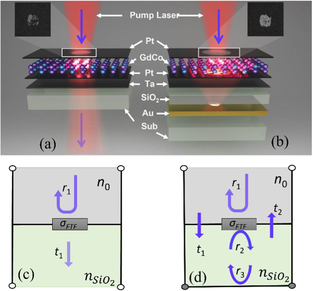
When an optical beam passes through one medium into another medium, reflections and transmissions will appear, simultaneously, and the well-known Fresnel equations can be used to calculate the reflection and transmission coefficients [29]. Due to the impedance mismatch of two transmission lines, similar phenomena can also exist in a circuit, when an electric signal propagates from one transmission line to another line with a different impedance [30,31]. Thus, an equivalent circuit model, which is convenient and easier to understand, can be used to calculate the optical beam propagation in two or more inhomogeneous optical media [32]. As shown in Fig. 1(a), an optical beam with a wavelength of impinges on an FTF composed of from the free space with refractive index . is the thickness of the GdCo layer, and the FTF is deposited on a substrate. The effect of each layer of the FTF will be explained in the following. From the theory of the equivalent circuit model, the free space and substrate are equivalent to two transmission lines with an impedance of and , respectively. Meanwhile, the FTF with an impedance of can be regarded as a load attached to the junction between the two transmission lines, as shown in Fig. 1(c). According to the Maxwell equations, the impedance has the relation of , where is the refractive index of the substrate. Then, the amplitude transmission and reflection coefficients can be calculated as [31]
Figure 1.Schematic of the AOS in (a) FTF and (b) CE-FTF. The FTF is composed of Pt/GdCo/Pt/Ta. Equivalent transmission line mode of (c) FTF and (d) CE-FTF. In the equivalent circuit model, the FTF is equivalent to a load with a conductivity of , and the added Au layer induces a short circuit. Insets show the magnetic domain state, where the black contrast corresponds to the initial magnetization, and the white contrast corresponds to a magnetization reversal.
To simplify Eqs. (1) and (2), the parameters , , and are introduced, where , , and is the complex conductivity of the FTF, which can be calculated by using the equivalent circuit method (see Appendix A and Appendix B). Figure 2(a) shows the conductivity of the FTF as a function of the thickness of the GdCo alloy. Then, the optical absorption of the FTF can be obtained as where and are the transmittance and reflectance of the incident beam, and , , respectively [31]. In Eq. (3), considering the limiting case, the maximal absorption is ), when and , concurrently. Therefore, the maximal absorption of the FTF cannot be larger than . As shown in Appendix C, COMSOL Multiphysics is employed to calculate the optical absorptions of each layer of the FTF under different thicknesses of GdCo alloy. We can find that the total absorption of the FTF is always less than 40% [Fig. 2(b)]. More importantly, the optical absorption of GdCo alloy, which works as the recording film, is less than 35%, and most of the laser energy is wasted, causing high energy consumption of AOS.
Figure 2.(a) Conductivity of the FTF as a function of the thickness of the GdCo alloy, and the thicknesses of Pt and Ta layers are 2 and 3 nm, respectively. (b) Optical absorption of each layer and the total absorption of the FTF under different thicknesses of the GdCo alloy. (c) Phase diagram of the optical absorption of the GdCo alloy as a function of its thickness and the thickness of the inserted dielectric layer . (d) Absorption of each layer of the CE-FTF under different thicknesses of the inserted dielectric layer with the thickness of .
To take advantage of the laser energy sufficiently and increase the optical absorption of GdCo alloy, a dielectric layer and an Au layer with a thickness of 20 nm are added between the FTF and the substrate, as shown in Fig. 1(b). A 20 nm Au layer is sufficient to meet the skin depth requirement at the pump laser frequency. The dielectric layer forms an optical cavity between the FTF and Au layer. In the new system, which is called “cavity-enhanced ferrimagnetic thin film” (CE-FTF) in the following, the Au layer can reflect the transmitting pump beam to the FTF again. Hence, by designing the thickness of the dielectric layer carefully, a resonance cavity with reflection coefficients of and can be obtained between the FTF and the Au layer. The equivalent circuit mode of the CE-FTF can be seen in Fig. 1(d). As shown in Fig. 1(d), because the thickness of the Au mirror is larger than its skin depth, the added Au layer causes a short circuit, where the reflection coefficient of the Au layer is . From the analysis before, the reflection coefficient of is
Based on the multiple interference theory (see Appendix D), the total reflection coefficient of the CE-FTF can be expressed as where is the propagation phase in the resonance cavity, and . Herein, is the free-space wavenumber, and . In Eq. (5), is the transmission coefficient of the pump beam from the inserted dielectric layer to the free space, and it is
Then, after simplification, the absorption of the CE-FTF is [31]
From Eq. (7), we can see that the absorption of this CE-FTF is a function of the conductivity of the FTF and the thickness of the dielectric layer, and it is easy to find that the maximal absorption of the CE-FTF is 100% when and . Because of the impedance mismatch, 100% perfect absorption is difficult to realize. However, as shown in Fig. 2(a), the thicknesses of Pt and Ta layers are selected as 2 and 3 nm, respectively, and the whole conductivity of the FTF can be tuned by changing the thickness of the GdCo alloy. Thus, by designing the parameters of the CE-FTF carefully, the absorption of the GdCo alloy can be enhanced as well.
Next, the optical absorption performance of the CE-FTF is surveyed under different thicknesses of the GdCo alloy and the inserted dielectric layer (). As shown in Fig. 2(c), at point , where the thicknesses of the GdCo alloy and the insert dielectric layer are and , the CE-FTF has a maximal optical absorption. Figure 2(d) shows the optical absorption of each layer of the CE-FTF under different thicknesses of the inserted dielectric layer with the thickness of . We can find the total absorption of the CE-FTF is larger than 80%; meanwhile, the absorption of the GdCo alloy layer has a maximal absorption of about 60% when . Compared with the single FTF [Fig. 2(b)], where only about 30% of the incident power is absorbed by the GdCo alloy when , the absorption has about twofold enhancement.
3. SAMPLE PREPARATION AND MEASUREMENT SETUP
After trading off the thickness of the GdCo alloy and the optical cavity performance, the samples are prepared. First, to find the net magnetization of the FTF [33,34], a series of 8 nm thickness alloys with different composition ratios of Gd ranging from to were grown by a magnetron sputtering system (TREC-MS-700) from Truth Equipment Corporation, TREC. As shown in Fig. 1(a), the FTF has the following multilayer structure: . To achieve a strong perpendicular magnetic anisotropy (PMA) and prevent oxidation, two layers of Pt with a thickness of 2 nm were deposited on the top and bottom of the GdCo alloy, respectively, and the Ta layer works as a buffer layer [33,35]. Then, the normalized magnetic hysteresis loops of the grown samples with different composition ratios are tested by the Kerr rotation in a MOKE system with the polar configuration at room temperature [34]. As shown in Fig. 3(a), the measurement results confirm that the FTFs have PMA when ranges from 16% to 24%. Figure 3(b) shows the coercive field under the different Gd content, which is extracted from Fig. 3(a), and we can obtain the at .
Figure 3.(a) Normalized hysteresis loops and (b) coercive field for the FTFs from MOKE with different composition ratios of Gd. (c) Static MOKE images of the PFTF and the CE-FTF with after illumination with different laser fluences.
Until now, the finally optimized structure and parameters of the CE-FTF can be confirmed, and it is . Then, the final samples were prepared. Before depositing the FTF, the Au layer and the inserted dielectric layer were prepared first by atomic layer deposition. To explore the effect of the inserted dielectric layer, a series of samples with the different inserted layers were grown, i.e., , 100, 150, and 200 nm, respectively. On the other hand, to make a comparison, a pure ferrimagnetic thin film (PFTF) without an Au layer and an inserted layer was prepared as well. By using a home-built static MOKE imaging system, as shown in Fig. 8 in Appendix F, the domain states of the samples after illumination with a single linearly polarized laser pulse are measured. Before illumination, a magnet with a magnetic field larger than the was applied to initialize the magnetization state of the sample. Figure 3(c) shows the magnetization of the PFTF and the CE-FTF with after illumination with different laser fluences, and the domain state can be distinguished by the white and black contrasts in the MOKE image. In Fig. 3(c), as for the PFTF, we can find almost no domain state switches when the laser fluence is less than ; as for the CE-FTF with , the domain state can be switched at the fluence of . With the increase of the laser fluence, the switching area is larger, and the CE-FTF can achieve almost a uniform magnetization switching when the fluence is , while it is about for the PFTF. All the MOKE images of the samples after illumination with different laser fluences are shown in Fig. 9 in Appendix G. Compared with the other results, it is also clear to find that the four CE-FTFs have little switching fluence, which is reduced by about 50%.
4. ULTRAFAST MAGNETIZATION DYNAMICS OF THE CE-FTF
Figure 4.Normalized ultrafast magnetization dynamics of (a) the CE-FTF with and (b) the PFTF triggered by the pump beam with different fluences. (c) The normalized ultrafast magnetization dynamics of the PFTF and the four CE-FTFs measured at under different laser fluences. (d) The normalized initial ultrafast magnetization dynamics of the PFTF triggered at the laser fluence of and the four CE-FTFs triggered at the laser fluence of , respectively. Here, , , , , , , , , , , , and .
We also explore the normalized ultrafast magnetization dynamics of the PFTF and the four CE-FTFs measured at , as shown in Fig. 4(c); they are extracted from Figs. 4(b) and 11 in Appendix I. We can find that all the four CE-FTFs have a lower laser fluence to reverse the magnetization, which means that the CE-FTFs have a higher efficiency of AOS. More importantly, the CE-FTF with has the highest efficiency at the same laser fluence. From Table 1, in Figs. 4(a) and 11, regardless of the TF or the SMR, we can see that the CE-FTF with has the preponderance of lower energy consumption and the highest magnetization reversal efficiency, which is the best for AOS.
5. PHOTOTHERMAL EFFECT DURING THE ULTRAFAST MAGNETIZATION REVERSAL
To demonstrate the magnetization manipulation process and certify the photothermal effect in the laser heating of the samples, the two-temperature model is applied to demonstrate the electronic and phonon temperature dynamics, as shown in Appendix E [36]. Figure 5 shows the electron and phonon temperatures of the PFTF and the four CE-FTFs under the same fluence. We can see that the electron and the phonon temperatures are increased from room temperature to the maximum after the pump of the laser beam; then, they both relax back to room temperature. We can also find that the electron and phonon temperatures of the four CE-FTFs are larger than those of the PFTF; they are also easier to reach their maximum temperature within about 0.5 ps. In addition, the CE-FTF with is the easiest to reach the maximum temperature, which is because it has a largest optical absorption. Figure 4(d) shows the normalized initial ultrafast magnetization dynamics of the four CE-FTFs triggered at the laser fluence of and PFTF triggered at the laser fluence of , respectively. In Fig. 4(d), two different behaviors, i.e., ultrafast demagnetization and rapid magnetization relaxation, can clearly be distinguished, and the ultrafast demagnetization is within about 0.5 ps. Meanwhile, the CE-FTF with has the largest demagnetization than other samples, and the PFTF and CE-FTF with have almost the same trend of magnetization dynamics because they have almost the same effective optical absorption. These results are well in account with the simulation of the two-temperature model. Thus, we can say that the CE-FTFs, especially the CE-FTF with , have an enhancement in photothermal effect, which induces the lower consumed time of AOS.
Figure 5.Calculated (a) electron temperature and (b) phonon temperature of the PFTF and the four CE-FTFs under the same laser fluence.
In summary, a cavity-enhanced AOS, which is composed of a GdCo alloy and a dielectric layer deposited on an Au layer, is proposed in this paper. The equivalent circuit model is employed to explore the optical absorption of the CE-FTF; further, by optimizing the thickness of the inserted dielectric layer of the cavity and the thickness of the GdCo alloy, the energy consumed by AOS is reduced by about 50%. The optimized structure and parameters of the CE-FTF, which is , are confirmed and prepared as well. We verify that the multilayer structure has a strong PMA and can achieve a uniform magnetization switching with a laser fluence less than , which is reduced by about 50% than the PFTF. A TR-MOKE system is used to test the performance of the samples precisely, and it once more affirms the low energy consumption of the CE-FTF. In addition, the magnetization switching speed, which is promoted, is also confirmed. The two-temperature model certifies that the enhancement in photothermal effect of the CE-FTF leads to a higher efficiency of magnetization switching. These excellent performances of CE-FTF make AOS an ideal way for energy-effective and fast magnetic recording and pave the way for its practical application.
APPENDIX A: COMPLEX CONDUCTIVITY OF EACH LAYER OF THE FTF
For the FTF, the effective permittivity of each layer has the relationship of , where is the complex conductivity, is the permittivity of vacuum, and is the frequency of the incident beam [37]. The effective permittivity of each layer is also the square of their refractive indexes. From Refs. [21,36], the complex refractive indexes of each layer are , , and , respectively. Thus, the complex conductivity of GdCo, Pt, and Ta layer is , , and , respectively.
APPENDIX B: EQUIVALENT CIRCUIT METHOD FOR CALCULATING COMPLEX CONDUCTIVITY OF THE FTF
From Ohm’s law, the incident beam with electric field will induce a current density in a conducting layer; if the thickness of the conducting layer is much smaller than its skin depth, the impedance of the conducting layer can be written as [30]. For the FTF composed of Pt/GdCo/Pt/Ta, four currents can be induced by the input beam, and the total current corresponds to a current through the four shunting impedances as shown in Fig. 6. Then, the total impedance of the FTF can be calculated by the impedance of each layer, which is given by [30]where , , and are the impedance of Pt layer, GdCo layer, and Ta layer, respectively. The complex conductivity of the FTF , where is the total thickness of the FTF. Thus, by changing the thickness of the GdCo alloy, the total thickness of the FTF will be changed, leading to the change of the . Figure 2(a) shows the real and imaginary components of the complex conductivity of the FTF as a function of the thickness of GdCo alloy.
Figure 6.Equivalent circuit mode of the FTF, and the four-layer spin films can be regarded as four parallel circuits.
APPENDIX C: OPTICAL ABSORPTION OF EACH LAYER OF THE FTF
The optical absorption of each layer of the FTF can be calculated from the ratio of the power dissipated as follows [38]: where is the power dissipation density, is the imaginary part of the permittivity of the FTF, is the electric field in the FTF, and is the electric field of the incident beam on an area . Figure 2(b) shows the absorption of each layer and the total absorption of the FTF under the different thicknesses of the GdCo alloy.
APPENDIX D: MULTIPLE INTERFERENCE THEORY
When the pump beam with electric field illuminates the CE-FTF, part of the optical beam will be reflected with a reflection coefficient , and part of the beam will transmit into the inserted layer with a transmission coefficient (Fig. 7). The latter one will continue propagation and be reflected by the Au mirror. Then, it will transmit into the air with a transmission coefficient or be reflected by the FTF with a reflection coefficient . Thus, the total reflection coefficient of the CE-FTF will be , where is the electric field of the reflected or transmitted beam, as shown in Fig. 7, and , , and [39]. After simplification, the total reflection coefficient of the CE-FTF can be obtained as [40]
Figure 7.Schematic of multiple reflections and interference model of the CE-FTF.
APPENDIX E: TWO-TEMPERATURE MODEL OF THE PHOTOTHERMAL EFFECT
The two-temperature model is applied to simulate the photothermal effect, and the dynamic temperature of the electron and phonon can be calculated. The two-temperature model is described by the following differential equations [17,36]:Here, and are the electron and phonon temperatures. is the electron-phonon coupling constant, and it is . is the room temperature, and it is 298 K. is the heat diffusion constant, and it is . and are the electron and phonon heat capacities and with , , respectively. describes the amount of laser energy absorbed by the sample, and ms−1 for the PFTF. is the laser fluence. is the laser pulse duration, and it is 35 fs. We should point out that, for the CE-FTF, because the absorption of the pump laser is enhanced, should be larger during the simulation. According to Figs. 2(a) and 2(c), the should be larger about 1.46, 1.9, 2.02 and 1.15 times for the four CE-FTFs, respectively. Figure 5 shows the electron and phonon temperatures of the PFTF and the four CE-FTFs under the same fluence. In Fig. 5, we can see that the electron and the phonon temperatures are increased from room temperature to the maximum after the pump of the laser beam; then, they both relax back to room temperature. Within 0.5 ps, can reach its maximum. We can also find that the CE-FTFs have a shorter time to reach the maximum temperature of the electron and phonon higher than the PFTF. Further, the electron and phonon temperatures of the four CE-FTFs are larger than those of the PFTF. Among the four CE-FTFs, the CE-FTF with is the easiest to reach the maximum temperature of the electron and phonon.
APPENDIX F: STATIC MOKE IMAGING SYSTEM
Figure 8 shows the schematic of the home-built static MOKE imaging system. The pump beam comes from an amplified Ti: sapphire laser with repetition rate , wavelength 780 nm, and pulse duration . The half-wave plate and polarizer P0 are used to tune the pump power.
APPENDIX G: STATIC MOKE IMAGES OF THE PFTF AND CE-FTF
Figure 9 shows the magnetization of the PFTF and the CE-FTF with , 100, 150, and 200 nm after illumination with different laser fluences, respectively.
Figure 9.Static MOKE images of the PFTF and CE-FTF with , 100, 150, and 200 nm, respectively.
Figure 10 shows the schematic of the home-built static TR-MOKE system. The amplified Ti:sapphire laser is employed, and the laser beam is divided into the pump beam and probe beam with a beam splitter. The frequency of the probe beam is doubled by a BBO crystal.
APPENDIX I: NORMALIZED ULTRAFAST MAGNETIZATION DYNAMICS OF THE CE-FTF
Figure 11 shows the normalized ultrafast magnetization dynamics of the CE-FTF with , 100, 150, 200 nm triggered by the pump beam with different fluence.
Figure 11.Normalized ultrafast magnetization dynamics of the CE-FTF with (a) , (b) , (c) , and (d) triggered by the pump beam with different fluence. Here, , , , , , , , and .