
Wentao Qiu, Huihui Lu, Fadi Issam Baida, Maria-Pilar Bernal, "Ultra-compact on-chip slot Bragg grating structure for small electric field detection," Photonics Res. 5, 212 (2017)
- Photonics Research
- Vol. 5, Issue 3, 212 (2017)
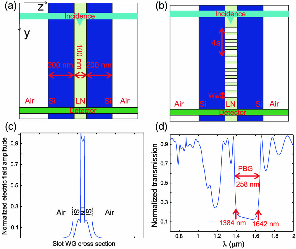
Fig. 1. (a) Sketch of 2D SWG considered in the 2D-FDTD simulations. (b) Sketch of 2D slot Bragg grating structure considered in the 2D-FDTD simulations. Period of grating a W air a = 340 nm W air = 200 nm N = 10
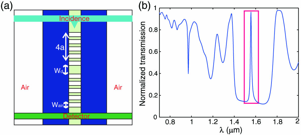
Fig. 2. (a) Sketch of 2D slot Bragg gating structure with a defect size of W d a W air a = 370 nm W air = 260 nm W d = 290 nm N = 5
Fig. 3. E-field amplitude distribution of E z 2(b) ] with excitation wavelength at (a) resonance peak wavelength of 1556 nm, (b) off-resonance wavelength of 1650 nm.
Fig. 4. (a) Sketch of 3D simulated structure. (b) Zero-order normalized transmission of 3D slot Bragg grating structure with different numbers of air grooves on each side of the F-P cavity.
Fig. 5. 3D-FDTD simulated zero-order normalized transmission with structure parameters as a = 380 nm W air = 260 nm H = 500 nm W si = 200 nm W s = 100 nm N = 7 W d
Fig. 6. 3D-FDTD zero-order normalized transmission of slot Bragg grating structure with parameters of a = 380 nm W air = 260 nm W si = 200 nm W s = 100 nm N = 7 H = 400 nm W d = 340 H = 700 nm W d = 320
Fig. 7. (a) Sketch of Bragg grating with silicon height larger than LN slot height. The air grooves etching depth equal to H si a = 380 nm W air = 260 nm H = 500 nm W si = 200 nm W s = 100 nm N = 7 W d = 380 nm H si
Fig. 8. (a) 3D FDTD normalized transmission calculated by Poynting energy flux at the output of the WG with parameters of H = 700 nm a = 380 nm W air = 260 nm W d = 340 nm N = 7 Δ n λ res Δ n
|
Table 1. PBG Size of 10 Air Grooves, a = 340 nm W air
|
Table 2. PBG Center Varying with a W air W air / a
|
Table 3. Resonance Properties Versus the Defect Size W d
|
Table 4. Resonance Properties Versus the Number of Air Grooves N


Set citation alerts for the article
Please enter your email address

© Copyright 2018-2021 | Chinese Laser Press. All Rights Reserved 沪ICP备15018463号-20