• Photonics Research
  • Vol. 5, Issue 6, 604 (2017)
Linbao Luo1, Kuiyuan Wang1, Caiwang Ge1, Kai Guo2, Fei Shen2, Zhiping Yin1、2, and Zhongyi Guo2、*
Author Affiliations
  • 1School of Electronic Science and Applied Physics, Hefei University of Technology, Hefei 230009, China
  • 2School of Computer and Information, Hefei University of Technology, Hefei 230009, China
  • show less
    DOI: 10.1364/PRJ.5.000604 Cite this Article Set citation alerts
    Linbao Luo, Kuiyuan Wang, Caiwang Ge, Kai Guo, Fei Shen, Zhiping Yin, Zhongyi Guo. Actively controllable terahertz switches with graphene-based nongroove gratings[J]. Photonics Research, 2017, 5(6): 604 Copy Citation Text show less
    Schematic of a uniform graphene-based grating structure: a graphene monolayer on a uniform silicon grating structure with PMMA as the interlayer. p is the grating period, w1 and w2 denote the widths of nongroove parts and groove parts of the grating, w2 is fixed at 30 nm in our work, and d1 and d2 are the depths of graphene sheet to nongroove and groove parts, respectively.
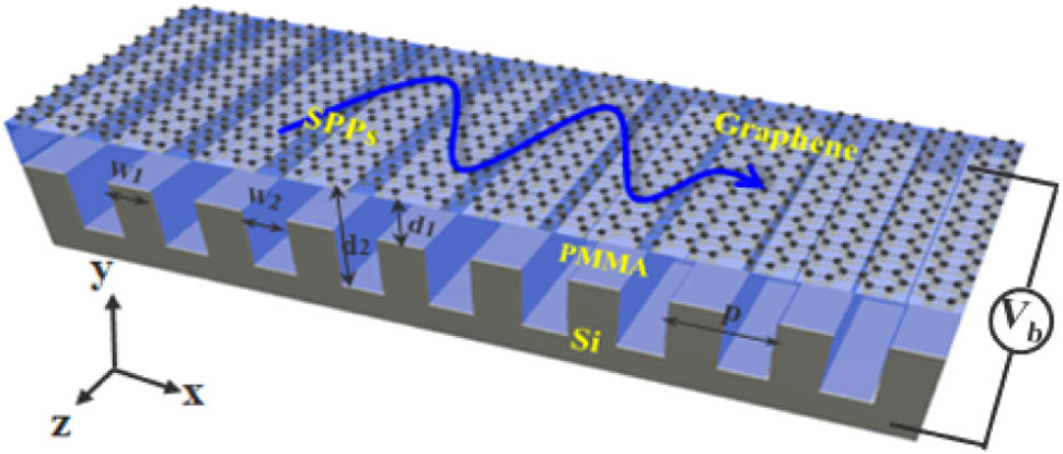
    Fig. 1. Schematic of a uniform graphene-based grating structure: a graphene monolayer on a uniform silicon grating structure with PMMA as the interlayer. p is the grating period, w1 and w2 denote the widths of nongroove parts and groove parts of the grating, w2 is fixed at 30 nm in our work, and d1 and d2 are the depths of graphene sheet to nongroove and groove parts, respectively.
    Real parts of the effective refractive index (neff) of SPP modes supported by the graphene monolayer, (a) as the function of frequency and the PMMA spacer depth d=d1=d2 with a constant gate voltage of Vb=60 V, and (b) as the function of frequency and the influence of the gate voltage Vb with constant PMMA spacer (d=d1=d2=50 nm).
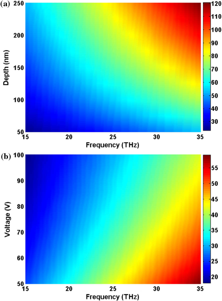
    Fig. 2. Real parts of the effective refractive index (neff) of SPP modes supported by the graphene monolayer, (a) as the function of frequency and the PMMA spacer depth d=d1=d2 with a constant gate voltage of Vb=60  V, and (b) as the function of frequency and the influence of the gate voltage Vb with constant PMMA spacer (d=d1=d2=50  nm).
    (a) Dispersion curves for different nongroove parts’ widths in the graphene-based uniform grating structure. (b) Dependence of slow-down factor S on the excitation frequencies for different nongroove widths. In the calculations, d1=50 nm, d2=250 nm, w2=30 nm, Vb=60 V.
    Fig. 3. (a) Dispersion curves for different nongroove parts’ widths in the graphene-based uniform grating structure. (b) Dependence of slow-down factor S on the excitation frequencies for different nongroove widths. In the calculations, d1=50  nm, d2=250  nm, w2=30  nm, Vb=60  V.
    Schematic illustration of the graphene-based graded grating structure. Here, d1=50 nm, d2=250 nm, w2=30 nm, and Vb=60 V. The nongroove width increases linearly from 30 to 65 nm with a step of Δ=1 nm; in our simulations, the width of the whole structure along the x axis is 2760 nm.
    Fig. 4. Schematic illustration of the graphene-based graded grating structure. Here, d1=50  nm, d2=250  nm, w2=30  nm, and Vb=60  V. The nongroove width increases linearly from 30 to 65 nm with a step of Δ=1  nm; in our simulations, the width of the whole structure along the x axis is 2760 nm.
    (a) Trapping position as a function of cutoff frequency. (b) Electric field distributions of |Ey|2 in the x–y plane of the graphene graded grating structure in Fig. 4 for incident wavelengths of 9, 9.5, and 10 μm, respectively. (c) Corresponding normalized field intensities distribution 2 nm above the graphene surface. (d) The slow-down factor S as a function of trapping position for different operating wavelength.
    Fig. 5. (a) Trapping position as a function of cutoff frequency. (b) Electric field distributions of |Ey|2 in the xy plane of the graphene graded grating structure in Fig. 4 for incident wavelengths of 9, 9.5, and 10 μm, respectively. (c) Corresponding normalized field intensities distribution 2 nm above the graphene surface. (d) The slow-down factor S as a function of trapping position for different operating wavelength.
    (a) Dispersion curves for w1=30 nm and w1=65 nm with different gate voltages (Vb=60 V and Vb=80 V). (b) Trapping position as a function of frequency for different gate voltages. (c) Electric field distributions of |Ey|2 in the x–y plane of the structure in Fig. 4 for 10 μm of Vb=40, 60, and 80 V, respective.
    Fig. 6. (a) Dispersion curves for w1=30  nm and w1=65  nm with different gate voltages (Vb=60  V and Vb=80  V). (b) Trapping position as a function of frequency for different gate voltages. (c) Electric field distributions of |Ey|2 in the xy plane of the structure in Fig. 4 for 10 μm of Vb=40, 60, and 80 V, respective.
    Theoretical critical gate voltages needed to turn on the optical switching as a function of frequency at the position x=2760 nm (output position).
    Fig. 7. Theoretical critical gate voltages needed to turn on the optical switching as a function of frequency at the position x=2760  nm (output position).
    Electric field distributions of |Ey|2 in the x–y plane of the modified structure for 10 μm at Vb=40, 60, and 80 V, respectively. White lines mark the material boundaries of the modified structure. The nongroove width increases linearly from 30 to 37 nm with a step of Δ=1 nm, and the groove width is fixed at 30 nm.
    Fig. 8. Electric field distributions of |Ey|2 in the xy plane of the modified structure for 10 μm at Vb=40, 60, and 80 V, respectively. White lines mark the material boundaries of the modified structure. The nongroove width increases linearly from 30 to 37 nm with a step of Δ=1  nm, and the groove width is fixed at 30 nm.
    Linbao Luo, Kuiyuan Wang, Caiwang Ge, Kai Guo, Fei Shen, Zhiping Yin, Zhongyi Guo. Actively controllable terahertz switches with graphene-based nongroove gratings[J]. Photonics Research, 2017, 5(6): 604
    Download Citation