Abstract
The photonic spin Hall effect (SHE) has been intensively studied and widely applied, especially in spin photonics. However, the SHE is weak and is difficult to detect directly. In this paper, we propose a method to enhance SHE with the guided-wave surface-plasmon resonance (SPR). By covering a dielectric with high refractive index on the surface of silver film, the photonic SHE can be greatly enhanced, and a giant transverse shift of horizontal polarization state is observed due to the evanescent field enhancement near the interface at the top dielectric layer and air. The maximum transverse shift of the horizontal polarization state with 11.5 μm is obtained when the thickness of Si film is optimum. There is at least an order of magnitude enhancement in contrast with the transverse shift in the conventional SPR configuration. Our research is important for providing an effective way to improve the photonic SHE and may offer the opportunity to characterize the parameters of the dielectric layer with the help of weak measurements and development of sensors based on the photonic SHE.1. INTRODUCTION
The photonic spin Hall effect (SHE) refers to the displacements perpendicular to the plane of incidence for the splitting of left- and right-handed circularly polarized components when the beam is reflected from or transmitted through a planar interface [1–5]. It is the optical analogy of the SHE in an electronic system in which spin electrons and an electric potential gradient correspond to the spin photons and refractive index gradient, respectively. Recently, the photonic SHE has attracted significant attention due to the physical sights and potential applications in nanophotonics [6]. It can be adopted to determine the optical thickness of a nanostructure [7], to identify the layer numbers of thin 2D materials [8], to characterize the material properties of magnetic thin film [9], chiral metamaterials [10,11], nano-metal film [12], and topological insulators [13,14].
To begin with the investigation of the photonic SHE in the interface of air and prism [15,16] and metallic reflection [17,18], it has been extended to complicated configurations and material systems, such as air–uniaxial crystal interface [19], left-handed materials [20], layered nanostructures [21], photon tunneling structure [22], and metasurfaces [23–25]. However, the photonic SHE corresponding spin-dependent splitting is a tiny phenomenon; in experiments, it is only dozens of nanometers in general cases [15,16]. Thus, some methods have been proposed to enhance the spin-dependent splitting in photonic SHE [26,27], such as Luo et al. who theorize an enhanced and switchable SHE of light near the Brewster angle on reflection and demonstrate it experimentally [26]. It is demonstrated that the spin-dependent splitting reaches 3200 nm near the Brewster angle, which is 50 times larger than previously reported values in refraction; Zhu et al. found that the SHE can be enhanced when a linearly polarized Gaussian beam transmits through a thin epsilon-near-zero slab due to the difference between the Fresnel transmission coefficients and [28]; Zhou et al. theoretically investigate the enhancement of the photonic SHE through considering the surface-plasmon resonance (SPR) effect in a three-layer structure composed of glass, metal, and air [29]. The authors found the SPR can be excited by a horizontal polarization beam, which will result in a huge transverse beam displacement far greater than the previous reported results observed at the air–glass interface. Tan et al. enhance the photonic SHE by taking advantage of long-range SPR (LRSPR). Under the optimal parameter setup, the largest transverse separation with a 632.8 nm incident Gaussian beam reaches 7.85 μm [30]. However, it is difficult to experimentally prepare the LRSPR structure; hence, it is difficult to experimentally demonstrate the giant photonic SHE’s phenomena.
In this paper, we theoretically investigate the photonic SHE in the guided-wave SPR (GWSPR). It is demonstrated that the photonic SHE can be greatly enhanced, and a giant transverse separation with 11 μm can be obtained by covering a layer of dielectric thin film with 10–15 nm having a high value of the real part of the dielectric function (silicon) on the conventional SPR configuration. There is at least an order of magnitude enhancement in contrast with the transverse shift in the conventional SPR configuration.
Sign up for Photonics Research TOC. Get the latest issue of Photonics Research delivered right to you!Sign up now
2. MODEL AND METHOD
As shown in Fig. 1, the GWSPR model consists of a four layer structure: the top layer is a prism; then a silver layer coating on the prism constitutes the conventional SPR structures. In order to enhance the photonic SHE, a thin silicon layer is coated on the silver; in the meantime, it can be adopted to prevent the silver from oxidizing in the air. In the next calculation, we choose the following parameters: , , , for wavelength , the thickness of sliver and silicon should be optimized to obtain the maximum transverse shifts.
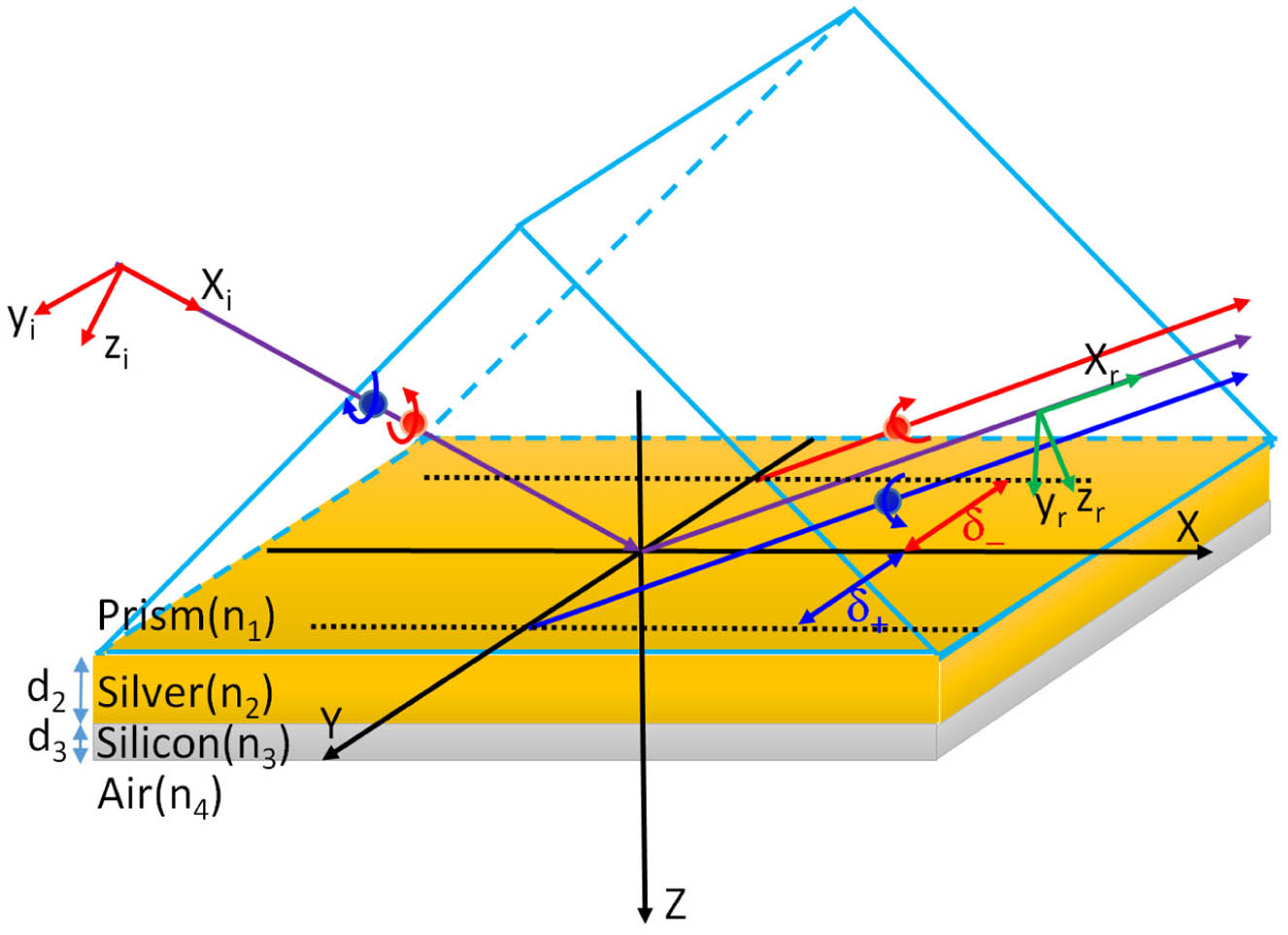
Figure 1.Schematic of the photonic SHE of a beam upon reflection of a GWSPR configuration. and indicate the transverse displacements for left- and right-circular polarization components, respectively.
A monochromatic Gaussian beam is incident from the prism, and it will be reflected by the silver layer due to the excitation of SPR. When there is only one silver dielectric layer adjacent to the prism, the structure is a Kretschmann configuration, which can support conventional SPR modes propagating along the metal–air interface [29]. The photonic SHE has been investigated by Zhou et al. [29]. However, the photonic SHE can be improved by the GWSPR configuration. The GWSPR configuration is similar to the SPR with an addition of a thin film between the metal layer and the cover material, which has been proposed to improve the sensitivity of the SPR sensor because of the evanescent field enhancement near the top layer-analyte interface [31,32]. The silicon film should be optimized to support the guided optical waves so that an asymmetric metal clad waveguide is produced.
In order to calculate the transverse displacements, a general beam propagation model using angular spectrum theory is employed. The incident Gaussian beam can be written as where is the beam waist, and and are the wave vector components in the and directions, respectively. In the spin basis set, the incident beam can be written as and ; here and present the horizontal and vertical polarization states, respectively. and denote the left- and right-handed circularly polarized components, respectively.
By matching the boundary condition, the reflected light beam can be given as [18,19] where is the wave vector in free space and is the reflected wave vector in the direction. and are the Fresnel reflection coefficients for - and -polarization states.
For the GWSPR configuration, the reflection coefficients can be written as where is the reflection coefficient at the interface of films 2, 3, and 4. It is obtained from where , , and are the reflection coefficients at the single interfaces, which is for the -polarization, and for the -polarization, where , respectively, and .
By making use of a Taylor series expansion based on the arbitrary spectrum components, and can be written as where .
If we confine our analysis to the first-order terms and neglect the high-order infinitesimal, then Eq. (7) can be written as According to Eqs. (2), (3), and (8), we can obtain the circular components of the reflected fields as where is the Rayleigh length. , , and are the coordinate components of Cartesian coordinate system at the reflected path.
The transverse displacements of reflected light can be defined as
Based on Eqs. (9)–(11), the transverse displacement of the reflected light beam can be expressed as
If the reflection coefficient and are insensitive to the incident angle , i.e., the FWHM of reflection coefficient under the angle coordinate is not narrow; then, the transverse displacement of the reflected light beam can be simplified by only considering the zero-order Taylor series in Eq. (8): which have been utilized to calculate the transverse displacement in simple structure, interface, or conventional SPR.
3. RESULTS AND DISCUSSION
Figure 2 describes the role of the metal film thickness and the incident angle in photonic SHE under . It can be found that the beam transverse displacements varying with the incident angles and the metal film thickness, and there are optimum parameters with the thickness of metal film due to the excitation of the surface plasmon polariton (SPPs). The enhanced SHE with SPPs has been investigated by Zhou et al. [25]; however, the authors only considered the zero-order Taylor series of the reflectance in Eq. (8); hence, Eqs. (14) and (15) have been employed to calculated the beam transverse displacements. In Fig. 2, we have considered the first-order Taylor series of the reflectance, so that Eqs. (12) and (13) have been employed to calculate the beam transverse displacements. It is clear that the maximum beam transverse displacement is about 1.2 μm, and the maximum beam transverse displacement is about 0.25 μm. Though the beam transverse displacement is larger in comparison with the SHE in the air–glass interface, the values are still tiny, which will restrict the potential applications. In the following research, we will study the enhancement of the transverse separation.

Figure 2.Dependences of transverse beam shifts on the metal film thickness and the incident angle with : (a) -polarization state; (b) -polarization state.
To study the influence of the thickness of Si film on the enhanced photonic SHE under the condition of SPR, we first analyze the influence of the silicon film on the SPR. Hence, in Fig. 3 we give the Fresnel reflectance changing with the incident angles when the silicon film thickness are 0, 8, and 12 nm, respectively. When the thickness of the Si film is zero, the behavior of the Fresnel reflective coefficients is the same as the condition in which a light beam reflects at the pure glass–metal–air interface [27]. It can be found that changes very little with the increasing incident angles and even keeps almost stable under the large incident angles; for the -polarization, has a narrow resonant dip near the resonant angle due to the excitation of the SPPs. According to Eqs. (14) and (15), the transverse displacement of the reflected light for the -polarization is proportional to the ratio of , the large ratio near the resonant dip leads to the enhancement of the transverse shifts of -polarization. However, it is found that the ratio is not big enough so that the maximum appears on a relatively limited range.
Figure 3.Dependences of the Fresnel reflectance and on the incident angle with the different thickness of silicon, where the silicon film thickness () is fixed to the three values: 0, 8, and 12 nm, when .
In order to enhance the ratio of and hence the transverse shifts ; we present a GWSPP structure by covering a tiny film of silicon on the metal film. As shown in Fig. 3, with the increasing Si film thickness, there are no significant changes of reflectance of -polarization; however, the Si film has a major impact on the reflectance of -polarization. Here the resonant angle is moving to the larger angle, and the FWHM of reflectance becomes broadened. Figure 4(a) shows the minimum value of and the corresponding resonant angle under different thicknesses of the Si film. It is demonstrated that, as continue to increase, the resonant angle [incident angle at ] change from 36° in the absence of silicon film to 69° with . However, the minimum reflectance of -polarization is decreased to a minimum value and then increased with the increase of . The optimum thickness of Si film is 12 nm for the minimum reflectance of -polarization. Compared with the reflectance of the SPR, the GWSPR can decrease the reflectance dip of the -polarization remarkably by covering a thin film with high refractive index on the silver film and increase the evanescent field near the interface of the top dielectric layer and air. Hence, the addition of a silicon layer with appropriate thickness can significantly improve the ratio of and enhance the transverse shift of photonic SHEs.
Figure 4.(a) Relation of minimum value of and incident angle at the minimum value of with the thickness of the Si film. (b) Value of changing with the incident angles under the Si film thickness are fixed to four values: 8, 10, 12, and 14 nm, where .
But what is the effect of the introduction of Si film on the ratio of and the transverse shifts ? To disclose the role of Si film on the transverse beam displacement, we will first analyze the variation of on the thickness of the Si film; as shown in Fig. 4(b), the value changing with the incident angles under the Si film thickness is fixed to the four values: 8, 10, 12, and 14 nm. It is found that the ratio is decreased to a minimum value and then increased with the increase of ; there is an optimum thickness to obtain the largest . It is clearer that the coupling of SPPs and waveguide mode due to the introduction of the Si film leads to the varying of ; hence, it is possible to enhance the transverse shift of photonic SHEs.
Equations (14) and (15) show that the value of the spin-dependent splitting mainly depends on the part , and the maximum spin-dependent splitting occurs when the is max, and then we can derivate the corresponding incident angle. Usually, when analysis Eq. (7), researchers only consider the zero-order terms and neglect the other order infinitesimal. In this paper, we meanwhile consider the first-order term. From Fig. 5, it can be found that the peak displacements of the transmitted beam are obtained near the resonant angles because the ratios are larger near these angles. Comparing Figs. 5(b) and 5(c) with 5(a), the transverse displacement is enhanced by a large margin with the introduction of Si film, which is far greater than the previous reported results observed at the air–glass interface or the air–metal–glass interface. Whether or not adding the Si film, the influence of the first-order term is especially obvious, which indicates that the first-order term cannot be neglected. Notably in regards to the narrow angle of reflectance, the influence of the first-order term is even more significant. According to Fig. 3, we find that the SPPs have a narrower angle of reflectance; hence, there is a significant reduction of transverse shift if we use the first-order term, as shown in Fig. 5(a). However, the influence of first-order term will become weaker and weaker due to the broader angle of reflectance with the introduction of Si film, as shown in Figs. 5(b) and 5(c). We also find that the first-order term will generate a dip for the transverse shifts of -polarization, which will suppress the transverse shifts of -polarization.
Figure 5.Photonic SHE in GWSPR model for - and -polarization state; we show the spin-dependent splitting varying with the incident angles under . Here, we choose three different thicknesses: (a) 0 nm; (b) 8 nm; (c) and the optimal thickness 12 nm.
In order to optimize the parameters to achieve the maximum transverse shifts of -polarization, in Fig. 6 we give the contour map of the transverse shifts of the -polarization state and -polarization state on the incident angle and the thickness of Si, respectively. Here we have adopted the first-order approximation to calculate the displacement. For -polarization input, a large positive transverse shift peak appears () when the incident angle and the thickness of Si due to the largest ratio . It can be observed that, when the thickness of Si is close to zero, that is the conventional SPR structure; thus, there is the minimum transverse shift peak in Fig. 6(a). Hence, the introduction of the Si film can significantly enhance the transverse shifts of the -polarization state. This phenomenon occurs due to the great enhancement of the ratio achieved by the coupled of the SPPs and waveguide mode. For -polarization input, as shown in Fig. 5(b), the maximum transverse shift peak appears when the incident angle in the absence of Si film. With the increasing thickness of Si film, the transverse shift is suppressed. In this case, the increasing ratio leads to the smaller and smaller transverse shift with the increasing angle of incidence. It can be concluded that the transverse shift is determined by the reflectance of light. Thus, by controlling the reflectance of incident light with the introduction of Si film, the SHE of reflectance light can be enhanced or suppressed and actively manipulated.
Figure 6.Dependence of the displacements (a) -polarization state and (b) -polarization state on the incident angle and the thickness of Si.
4. CONCLUSION
In summary, we analyzed the enhanced photonic SHE, while the coupled SPPs and waveguide mode is excited. The enhancement is affected by the thicknesses of the silicon layer and the silver layer. The maximum transverse shifts of the -polarization state with 11.5 μm have been obtained by optimizing the parameters of the thicknesses of the silicon layer and the silver layer. Our results are much greater than formerly reported values. Thus, by manipulating the properties of the added Si film, the SHE of reflectance light can be enhanced or suppressed. Our findings also will likely have potential applications for developing nanophotonic devices based on spin optics and the control of photons.
References
[1] M. Onoda, S. Murakami, N. Nagaosa. Hall effect of light. Phys. Rev. Lett., 93, 083901(2004).
[2] S. Murakami, N. Nagaosa, S. Zhang. Dissipationless quantum spin current at room temperature. Science, 301, 1348-1351(2003).
[3] J. Sinova, D. Culcer, Q. Niu, N. A. Sinitsyn, T. Jungwirth, A. H. Macdonald. Universal intrinsic spin Hall effect. Phys. Rev. Lett., 92, 126603(2004).
[4] J. Wunderlich, B. Kaestner, J. Sinova, T. Jungwirth. Experimental discovery of the spin-Hall effect in Rashba spin-orbit coupled semiconductor systems. Phys. Rev. Lett., 94, 047204(2005).
[5] K. Y. Bliokh, F. J. Rodríguez-Fortuño, F. Nori, A. V. Zayats. Spin-orbit interactions of light. Nat. Photonics, 9, 796-808(2015).
[6] X. Ling, X. Zhou, K. Huang, Y. Liu, C.-W. Qiu, H. Luo, S. Wen. Recent advances in the spin Hall effect of light. Rep. Prog. Phys., 80, 066401(2017).
[7] X. Ling, X. Zhou, H. Luo, S. Wen. Steering far-field spin-dependent splitting of light by inhomogeneous anisotropic media. Phys. Rev. A, 86, 053821(2012).
[8] X. Zhou, X. Ling, H. Luo, S. Wen. Identifying graphene layers via spin Hall effect of light. Appl. Phys. Lett., 101, 251602(2012).
[9] X. Checoury, D. Neel, P. Boucaud, C. Gesset, H. Girard, S. Saada. Nanocrystalline diamond photonics platform with high quality factor photonic crystal cavities. Appl. Phys. Lett., 101, 171115(2012).
[10] H. Wang, X. Zhang. Unusual spin Hall effect of a light beam in chiral metamaterials. Phys. Rev. A, 83, 053820(2011).
[11] J. Duan, H. Guo, S. Dong, T. Cai, W. Luo, Z. Liang, Q. He, L. Zhou, S. Sun. High-efficiency chirality-modulated spoof surface plasmon meta-coupler. Sci. Rep., 7, 1354(2017).
[12] X. Ling, X. Zhou, S. Wen. Steering far-field spin-dependent splitting of light by inhomogeneous anisotropic media. Phys. Rev. A, 86, 053824(2012).
[13] X. Zhou, J. Zhang, X. Ling, S. Chen, H. Luo, S. Wen. Photonic spin Hall effect in topological insulators. Phys. Rev. A, 88, 053840(2013).
[14] P. Wang, W. Li, Q. Liu, X. Jiang. Giant topological magnetoelectric and optical Hall effects for a topological insulator as a defect in photonic crystals. Phys. Rev. A, 90, 015801(2014).
[15] O. Hosten, P. Kwiat. Observation of the spin hall effect of light via weak measurements. Science, 319, 787-790(2008).
[16] Y. Qin, Y. Li, H. He, Q. Gong. Measurement of spin Hall effect of reflected light. Opt. Lett., 34, 2551-2553(2009).
[17] N. Hermosa, A. M. Nugrowati, A. Aiello, J. P. Woerdman. Spin Hall effect of light in metallic reflection. Opt. Lett., 36, 3200-3202(2011).
[18] X. Zhou, Z. Xiao, H. Luo, S. Wen. Experimental observation of the spin Hall effect of light on a nano-metal film via weak measurements. Phys. Rev. A, 85, 043809(2012).
[19] Y. Qin, Y. Li, X. Feng, Z. Liu, H. He, Y. Xiao, Q. Gong. Spin Hall effect of reflected light at the air-uniaxial crystal interface. Opt. Express, 18, 16832-16839(2010).
[20] H. Luo, S. Wen, W. Shu, Z. Tang, Y. Zou, D. Fan. Spin Hall effect of a light beam in left-handed materials. Phys. Rev. A, 80, 043810(2009).
[21] H. Luo, X. Ling, X. Zhou, W. Shu, S. Wen, D. Fan. Enhancing or suppressing the spin Hall effect of light in layered nanostructures. Phys. Rev. A, 84, 033801(2011).
[22] X. Zhou, X. Ling, Z. Zhang, H. Luo, S. Wen. Observation of spin Hall effect in photon tunneling via weak measurements. Sci. Rep., 4, 7388(2014).
[23] W. Luo, S. Xiao, Q. He, S. Sun, L. Zhou. Photonic spin Hall effect with nearly 100% efficiency. Adv. Opt. Mater., 3, 1102-1108(2015).
[24] X. Yin, Z. Ye, J. Rho, Y. Wang, X. Zhang. Photonic spin Hall effect at metasurfaces. Science, 339, 1405-1407(2013).
[25] W. Luo, S. Sun, H.-X. Xu, Q. He, L. Zhou. Transmissive ultrathin Pancharatnam-Berry metasurfaces with nearly 100% efficiency. Phys. Rev. Appl., 7, 044033(2017).
[26] H. Luo, X. Zhou, W. Shu, S. Wen, D. Fan. Enhanced and switchable spin Hall effect of light near the Brewster angle on reflection. Phys. Rev. A, 84, 043806(2011).
[27] L. Kong, X. Wang, S. Li, Y. Li, J. Chen, B. Gu, H. Wang. Spin Hall effect of reflected light from an air-glass interface around the Brewster’s angle. Appl. Phys. Lett., 100, 071109(2012).
[28] W. Zhu, W. She. Enhanced spin Hall effect of transmitted light through a thin epsilon-near-zero slab. Opt. Lett., 40, 2961-2964(2015).
[29] X. Zhou, X. Ling. Enhanced photonic spin Hall effect due to surface plasmon resonance. IEEE Photon. J., 8, 1-8(2016).
[30] X.-J. Tan, X.-S. Zhu. Enhancing photonic spin Hall effect via long-range surface plasmon resonance. Opt. Lett., 41, 2478-2481(2016).
[31] A. Lahav, M. Auslender, I. Abdulhalim. Sensitivity enhancement of guided-wave surface-plasmon resonance sensors. Opt. Lett., 33, 2539-2541(2008).
[32] A. Abbas, M. J. Linman, Q. Cheng. Sensitivity comparison of surface plasmon resonance and plasmon-waveguide resonance biosensors. Sens. Actuators B Chem., 156, 169-175(2011).


