• Acta Optica Sinica
  • Vol. 39, Issue 3, 0316001 (2019)
Yaqin Huang1, Yi Li1、2、*, Zhengpeng Li1, Jiangheng Pei1, Rong Tian1, Jin Liu1, Jianzhong Zhou1, Baoying Fang1, Xiaohua Wang1、3, and Han Xiao1、4
Author Affiliations
  • 1 School of Optical-Electrical and Computer Engineering, University of Shanghai for Science and Technology, Shanghai 200093, China
  • 2 Shanghai Key Laboratory of Modern Optical System, Shanghai 200093, China
  • 3 School of Electric and Information, Shanghai University of Electric Power, Shanghai 200090, China
  • 4 College of Medical Imaging, Shanghai University of Medicine & Health Sciences, Shanghai 201318, China;
  • show less
    DOI: 10.3788/AOS201939.0316001 Cite this Article Set citation alerts
    Yaqin Huang, Yi Li, Zhengpeng Li, Jiangheng Pei, Rong Tian, Jin Liu, Jianzhong Zhou, Baoying Fang, Xiaohua Wang, Han Xiao. Tunable Mid-Infrared Broadband Absorber Based on W/VO2 Square Nano-Pillar Array[J]. Acta Optica Sinica, 2019, 39(3): 0316001 Copy Citation Text show less
    Structural diagrams of absorber. (a) Three-dimensional view of unit cell; (b) top view of unit cell
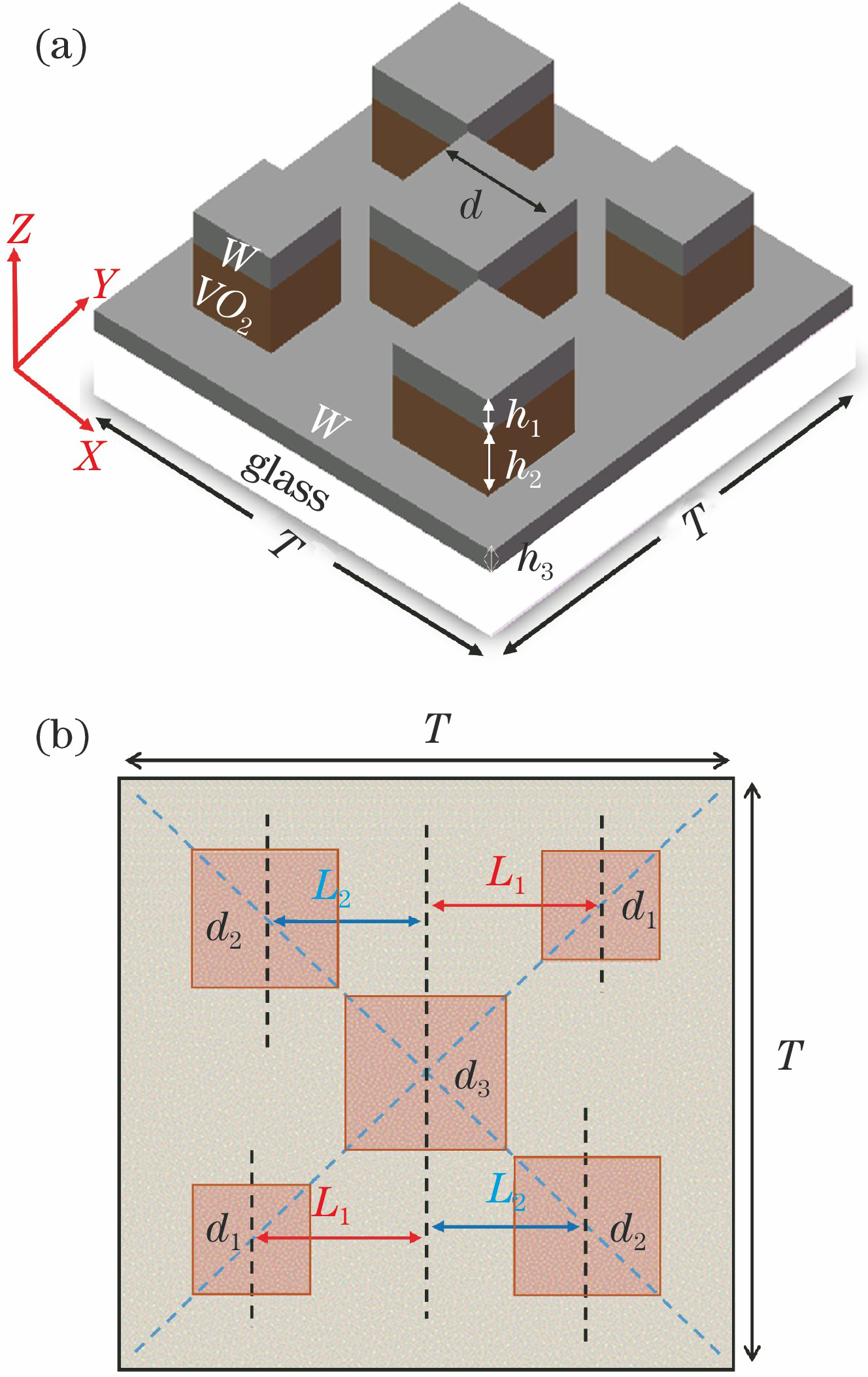
    Fig. 1. Structural diagrams of absorber. (a) Three-dimensional view of unit cell; (b) top view of unit cell
    Effects of structural parameters of absorber on absorption characteristics. (a) Dielectric layer VO2 thickness h2; (b) nano-pillar side length d3; (c) nano-pillar side length d1; (d) nano-pillar side length d2; (e) top W film thickness h1; (f) period T; (g) distance L1 between nano-pillar with side length d1 and center line of unit; (h) distance L2 between nano-pillar with side length d2 and center line of unit
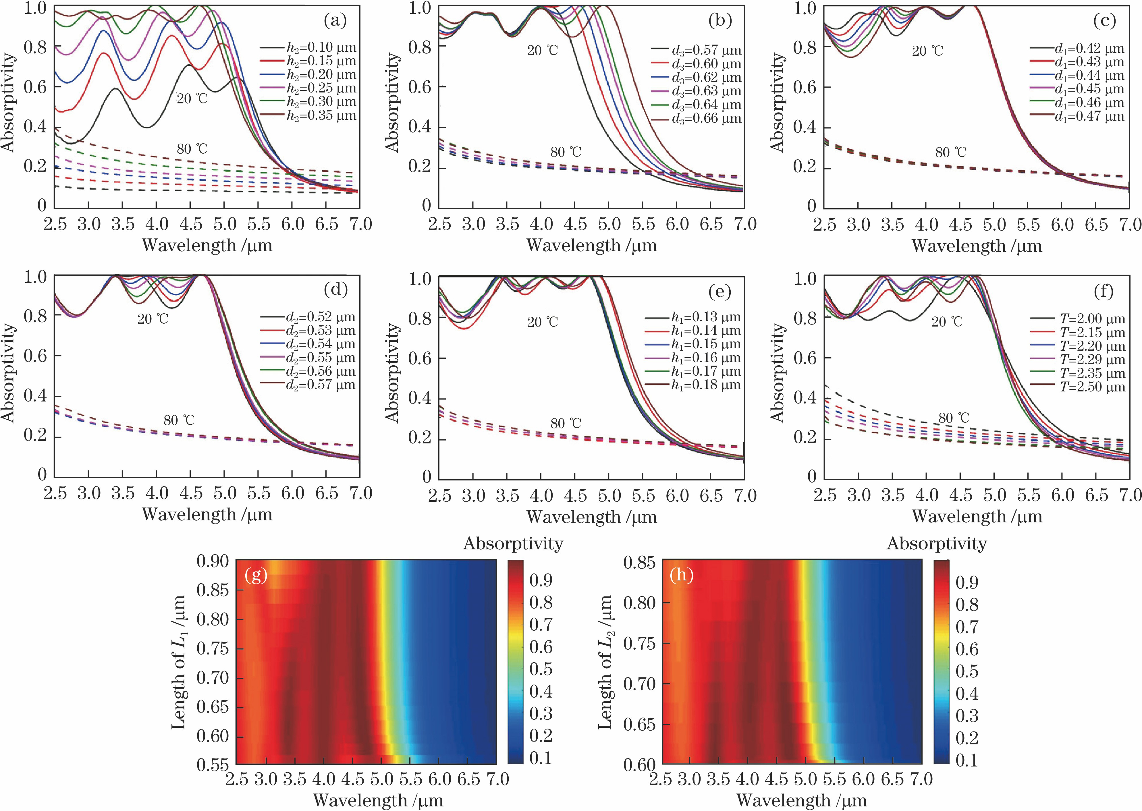
    Fig. 2. Effects of structural parameters of absorber on absorption characteristics. (a) Dielectric layer VO2 thickness h2; (b) nano-pillar side length d3; (c) nano-pillar side length d1; (d) nano-pillar side length d2; (e) top W film thickness h1; (f) period T; (g) distance L1 between nano-pillar with side length d1 and center line of unit; (h) distance L2 between nano-pillar with side length d2 and center line of unit
    Absorptivity of absorber versus temperature
    Fig. 3. Absorptivity of absorber versus temperature
    Magnetic field distributions of the X-Y section of the absorber at the center of VO2 dielectric layer (Z=0.25 μm). (a) 20 ℃, λ=3 μm; (b) 20 ℃, λ=4 μm; (c) 20 ℃, λ=5 μm; (d) 80 ℃, λ=3 μm; (e) 80 ℃, λ=4 μm; (f) 80 ℃, λ=5 μm
    Fig. 4. Magnetic field distributions of the X-Y section of the absorber at the center of VO2 dielectric layer (Z=0.25 μm). (a) 20 ℃, λ=3 μm; (b) 20 ℃, λ=4 μm; (c) 20 ℃, λ=5 μm; (d) 80 ℃, λ=3 μm; (e) 80 ℃, λ=4 μm; (f) 80 ℃, λ=5 μm
    Absorptivity of the absorber at 20 °C. (a) Different polarization angles; (b) different incident angles for TM polarization and TE polarization
    Fig. 5. Absorptivity of the absorber at 20 °C. (a) Different polarization angles; (b) different incident angles for TM polarization and TE polarization
    Yaqin Huang, Yi Li, Zhengpeng Li, Jiangheng Pei, Rong Tian, Jin Liu, Jianzhong Zhou, Baoying Fang, Xiaohua Wang, Han Xiao. Tunable Mid-Infrared Broadband Absorber Based on W/VO2 Square Nano-Pillar Array[J]. Acta Optica Sinica, 2019, 39(3): 0316001
    Download Citation