
Lianping Hou, Song Tang, John H. Marsh. Monolithic DWDM source with precise channel spacing[J]. Journal of Semiconductors, 2021, 42(4): 042301
- Journal of Semiconductors
- Vol. 42, Issue 4, 042301 (2021)
Abstract
1. Introduction
New approaches are needed for manufacturing optoelectronic hardware, particularly in the access network where increasing data rates need to be provided at low cost. For example, standards for the next generation of passive optical networks (PONs) envisage dense wavelength division multiplexing (DWDM) supporting aggregate data rates of 40 Gb/s[
The grating period Λ of each laser is related to the Bragg wavelength through
We have used ridge waveguides with conventional sampled Bragg gratings (C-SBG) etched into the side-walls[
2. Device structure and fabrication
The structure of the epitaxial layers[
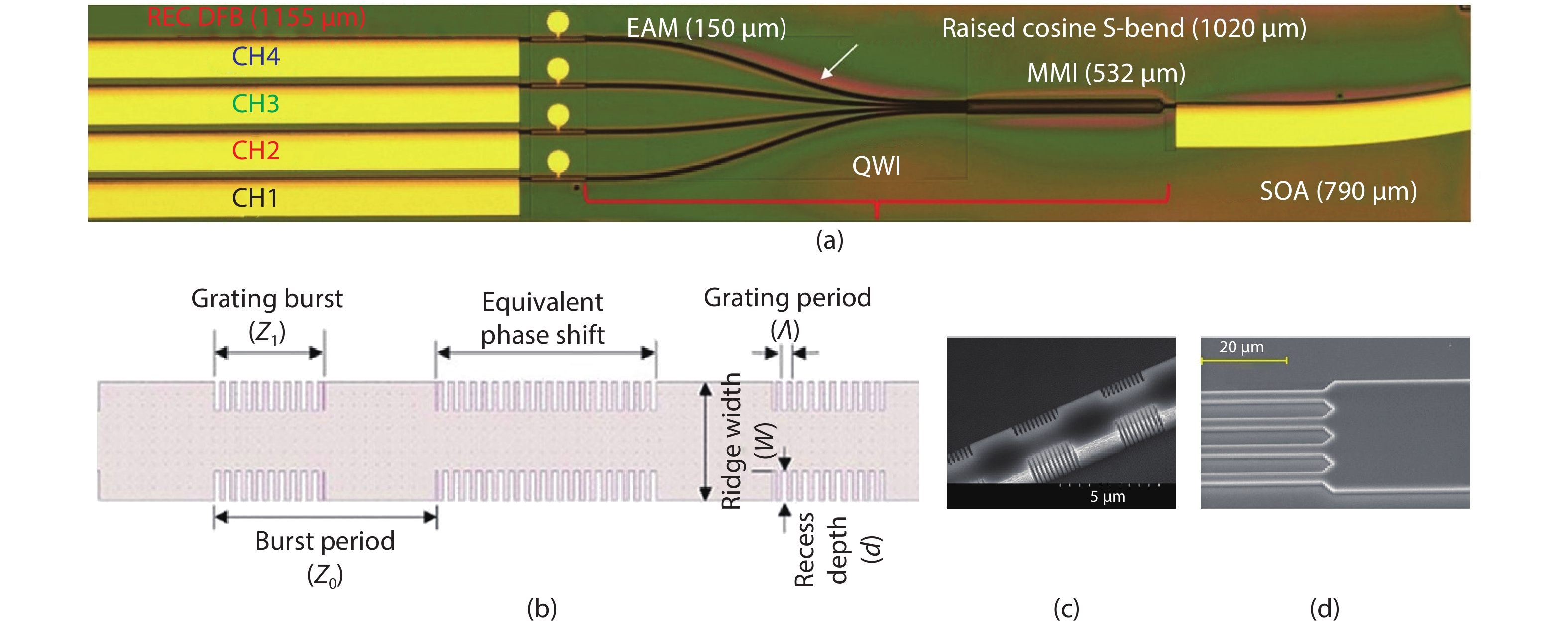
Fig. 1(a) shows an optical microscope picture of a single chip, together with its dimensions. The pitch between adjacent lasers was 125 μm and their ridge width was 2.5 μm. QWI was used to widen the bandgap in the MMI and S-bends by around 100 nm. The 4 × 1 MMI coupler was 30 μm-wide and 532 μm-long [Fig. 1(d)]. The raised cosine S-bends were 1020 μm-long. To minimize facet reflectivity, the SOA was fabricated as a curved waveguide terminating at an angle of 10° to the facet normal. The SOA compensated for the intrinsic loss of 6 dB of the 4 × 1 MMI coupler and allowed the output power to be increased to > 10 dBm. The SOA also can be used to shutter the output when the wavelength is being switched [
![]()
Figure 1.(Color online) (a) DWDM source optical micrograph. (b) Illustration and relevant dimensions of the side-wall sampled grating with equivalent phase shift. (c) SEM picture of the side-wall sampled gratings. (d) Input part of the MMI coupler.
![]()
Figure 2.(Color online) The simulated C-SBG power reflectivity of the four channels.
![]()
Figure 3.(Color online) Measured from SOA side of the four channels (a) wavelengths vs
Simulations of the power reflectivity of the sampled gratings are shown in Fig. 2, in which the waveguide internal loss of 15 cm−1 has been taken into account. As noted above, the operating wavelengths of the lasers were determined by the +1st order reflection peaks and lay between 1556.54 and 1554.14 nm with a spacing of 0.8 nm. The −1st order wavelengths lie around 1410 nm where the modal gain is too low to support laser operation.
3. Device performance
The DFB laser threshold currents were ~100 mA corresponding to a current density of 3.46 kA/cm2, which is slightly higher than that of traditional buried grating ridge waveguide DFB lasers (2.29 kA/cm2)[
In Fig. 3(a), it can be seen that the DFB laser wavelength can be tuned by changing its drive current, and the tuning rate was determined to be 0.013 nm/mA. When the current is held constant, the tuning coefficient is around 0.1 nm/K over the range −5 to +70 °C. The current tuning range of each DFB laser was around 2.3 nm, and the largest wavelength difference between DFB1 and DFB4 was 4.61 nm. During current tuning, no mode hopping was observed.
![]()
Figure 4.(Color online) (a) Measured lasing wavelength of the four channels and the curve of its linear fitting. (b) Residual of the lasing wavelength and SMSR of the four channels. (c) Measured ER from coupled SMF of the four channels. (d) Channel 1 small signal E/O response at different
With IDFB = 300 mA (3Ith), ISOA = 150 mA, and VEAM = 0 V, the optical spectra measured at 20 °C from the SOA side are shown in Fig. 3(b). The lasing wavelengths of the four DFB lasers were 1558, 1557.27, 1556.62, 1555.64 nm with a wavelength spacing around 0.8 nm, very close to the simulations presented in Fig. 2 other than the measured wavelengths were redshifted due to heating at higher injection currents (300 mA).
The lasing wavelengths of the four channels from Fig. 3(b) and a linear fit with a gradient of −0.8 nm/CH are shown in Fig. 4(a). The residual error of the four channel lasing wavelengths after linear fitting of the lasing wavelengths versus the channel number is shown in Fig. 4(b). The residuals vary from −0.084 to 0.13 nm; the small magnitudes of the residuals are attributed to the precise control of the sampled grating periods, Z0, and grating pitch, Λ, offered by EBL. The residuals can be eliminated either by slightly varying the temperature (< 1.5 °C) using a separate heater in each channel or by changing the drive current (by tuning the current by < 10 mA out of 300 mA). The measured single-mode suppression ratios (SMSRs) are shown inFig. 4(b); all SMSRs exceed 33 dB, demonstrating excellent SLM operation of the DWDM source. By comparing the spectra from the SOA and DFB sides, it can be seen there is no degradation associated with the SOA.
![]()
Figure 5.Schematic structures of (a) C-SBG, (b) 2PS-SBG, (c) 3PS-SBG, and (d) 4PS-SBG.
The power coupled into a single mode fiber (SMF) for the four channels when IDFB = 300 mA, ISOA = 150 mA is shown in Fig. 4(c). The true maximum power from the SOA side should be more than 10 mW because the coupling efficiency to the SMF was less than 30%[
4. Multisection PS-SBG
As can be seen in Figs. 1(b) and 1(c), every sampled period of a C-SBG structure has a section where the grating is absent, which will reduce the κ value. Because the design uses ±1st-order reflections and a 50% sampling duty cycle, the effective κ is reduced to 1/π (~ 0.32) times that of the κ of a uniform grating[
![]()
Figure 6.(Color online) Simulated power reflection comparison between (a) uniform grating (UG) and C-SBG, (b) 2PS-SBG and C-SBG, (c) 3PS-SBG and C-SBG, (d) 4PS-SBG and C-SBG.
The characteristics of the reflection spectra of the C-SGB, 2PS-SBG, 3PS-SBG, and 4PS-SBG and their effective κ values compared with a uniform grating are summarized in Table 1.
Using a 2PS-SBG scheme with the 0th-order sidewall grating period set at 250 nm and the sampling periods ranging from 7.979 to 9.206 µm, an eight-channel DFB laser array was fabricated with 0.837 nm channel spacing and 0.059 nm residual, as shown in Fig. 7(b)[
![]()
Figure 7.(Color online) (a) Measured optical spectra of the 8-channel laser array at 100 mA (left to right, channels 1 to 8) and (b) 8-channel lasing wavelengths and the linear fitting.
Because multisection PS-SBGs have a higher κ value, it is possible to reduce the length of the DFB cavity with a corresponding reduction in the threshold current. The technique can also be used in future to fabricate directly modulated DFB lasers.
5. Conclusion
In summary, a 4-channel DWDM source suitable for use in PONs has been demonstrated by a combination of the REC, IEL, and QWI techniques. The device has an output power > 10 dBm and a channel spacing of 0.8 nm (100 GHz). The approach has the advantages of providing accurate control over the individual lasing wavelengths, offering a potentially high SLM manufacturing yield and low manufacturing costs. Using a C-SBG structure, the κ value is reduced to 0.32 times that of a uniform grating (assuming a sampling period duty cycle of 50%), but by using multisection PS-SBG designs, the κ value can be increased while maintaining precise control of the channel wavelength spacing of the DFB laser array. Based on a 2PS-SBG design, an 8-channel DFB laser array was fabricated using a single stage of EBL with a 0.837 nm channel spacing and 0.059 nm residual.
Acknowledegments
This work was supported by the U.K. Engineering and Physical Sciences Research Council (EP/R042578/1) and the National Science Foundation of China (61320106013). We would like to acknowledge the staff of the James Watt Nanofabrication Centre at the University of Glasgow for help in fabricating the devices.
References
[1]
[2] Sillard H Debrégeas, C Kazmierski. Challenges and advances of photonic integrated circuits. Comptes Rendus Physique, 9, 1055(2008).
[3] K Kudo, K Yashiki, T Sasaki et al. 1.55-
[4] Y Muroya, T Nakamura, H Yamada et al. Precise wavelength control for DFB laser diodes by novel corrugation delineation method. IEEE Photon Technol Lett, 9, 288(1997).
[5] Y C Shi, X F Chen, Y T Zhou et al. Experimental demonstration of eight-wavelength distributed feedback semiconductor laser array using equivalent phase shift. Opt Lett, 37, 3315(2012).
[6] Y C Shi, S M Li, X F Chen et al. High channel count and high precision channel spacing multi-wavelength laser array for future PICs. Sci Rep, 4, 7377(2015).
[7] C Z Sun, B Xiong, J Wang et al. Fabrication and packaging of 40-Gb/s AlGaInAs multiple-quantum-well electroabsorption modulated lasers based on identical epitaxial layer scheme. J Lightwave Technol, 26, 1464(2008).
[8] L P Hou, M Haji, R Dylewicz et al. Monolithic 45-GHz mode-locked surface-etched DBR laser using quantum-well intermixing technology. IEEE Photon Technol Lett, 22, 1039(2010).
[9] L P Hou, M Haji, R Dylewicz et al. 10-GHz mode-locked extended cavity laser integrated with surface-etched DBR fabricated by quantum-well intermixing. IEEE Photon Technol Lett, 23, 82(2011).
[10] L Hou, M Haji, J H Marsh. Mode locking at terahertz frequencies using a distributed Bragg reflector laser with a sampled grating. Opt Lett, 38, 1113(2013).
[11] L P Hou, P Stolarz, J Javaloyes et al. Subpicosecond pulse generation at quasi-40-GHz using a passively mode-locked AlGaInAs–InP 1.55-
[12] L P Hou, M Haji, J Akbar et al. AlGaInAs/InP monolithically integrated DFB laser array. IEEE J Quantum Electron, 48, 137(2012).
[13] H Ishii, K Kasaya, H Oohashi. Spectral linewidth reduction in widely wavelength tunable DFB laser array. IEEE J Sel Top Quantum Electron, 15, 514(2009).
[14] T Nakura, Y Nakano. LAPAREX-An automatic parameter extraction program for gain-and index-coupled distributed feedback semiconductor lasers, and its application to observation of changing coupling coefficients with currents. IEICE Trans Electron, 83, 488(2000).
[15] M Faugeron, M Tran, F Lelarge et al. High-power, low RIN 1.55-
[16] L Hou, M Haji, J Akbar et al. Low divergence angle and low jitter 40 GHz AlGaInAs/InP 1.55
[17] A Ramdane, F Devaux, N Souli et al. Monolithic integration of multiple-quantum-well lasers and modulators for high-speed transmission. IEEE J Sel Top Quantum Electron, 2, 326(1996).
[18] R Hanfoug, L Augustin, Y Barbarin et al. Reduced reflections from multimode interference couplers. Electron Lett, 42, 465(2006).
[19] R Weinmann, D Baums, U Cebulla et al. Polarization-independent and ultra-high bandwidth electroabsorption modulator in multiquantum-well deep-ridge waveguide technology. IEEE Photon Technol Lett, 8, 891(1996).
[20] J Kreissl, C Bornholdt, T Gaertner et al. Flip-chip compatible electroabsorption modulator for up to 40 Gb/s, integrated with 1.55
[21] J S Li, Y Cheng, Z W Yin et al. A multiexposure technology for sampled Bragg gratings and its applications in dual-wavelength lasing generation and OCDMA en/decoding. IEEE Photon Technol Lett, 21, 1639(2009).
[22] S Tang, L Hou, X Chen et al. Multiple-wavelength distributed-feedback laser arrays with high coupling coefficients and precise channel spacing. Opt Lett, 42, 1800(2017).

Set citation alerts for the article
Please enter your email address
© Copyright 2018-2021 | Chinese Laser Press. All Rights Reserved 沪ICP备15018463号-20