Andrew M. Armstrong1,*, Brianna A. Klein1, Andrew A. Allerman1, Albert G. Baca1..., Mary H. Crawford1, Jacob Podkaminer1,2, Carlos R. Perez1, Michael P. Siegal1, Erica A. Douglas1, Vincent M. Abate1 and Francois Leonard3|Show fewer author(s)
Abstract
AlGaN-channel high electron mobility transistors (HEMTs) were operated as visible- and solar-blind photodetectors by using GaN nanodots as an optically active floating gate. The effect of the floating gate was large enough to switch an HEMT from the off-state in the dark to an on-state under illumination. This opto-electronic response achieved responsivity at room temperature while allowing HEMTs to be electrically biased in the off-state for low dark current and low DC power dissipation. The influence of GaN nanodot distance from the HEMT channel on the dynamic range of the photodetector was investigated, along with the responsivity and temporal response of the floating gate HEMT as a function of optical intensity. The absorption threshold was shown to be controlled by the AlN mole fraction of the HEMT channel layer, thus enabling the same device design to be tuned for either visible- or solar-blind detection.1. INTRODUCTION
Visible- and solar-blind photodetectors serve many applications. Visible-blind detectors enable indoor non-line-of-sight communication, and solar-blind detectors find use for flame detection, biochemical pathogen detection, and outdoor non-line-of-sight communication [1]. Silicon avalanche photodiodes (APDs) or photomultiplier tubes (PMTs) are used for visible- or solar-blind applications, but they each have drawbacks. Photomultiplier tubes operate at high voltages that require bulky power supplies. Silicon APDs require cooling to achieve high detectivity and suffer high dark count rate [1]. Also, Si APDs and PMTs naturally absorb visible and UV radiation, so they require expensive optical filters to achieve a high visible rejection ratio (VRR) or solar rejection ratio (SRR).
Floating gate high electron mobility transistors (HEMTs) have been proposed and demonstrated for high-sensitivity photodetection with low-voltage operation and low dark count rate [2–4]. The concept is to localize a photogenerated electron or hole between the gate and channel of the HEMT [5]. If the localization medium is of high crystal quality and has a high potential barrier, the trapped carrier can be long-lived. The localized charge acts as a floating gate that exerts electrostatic potential on the channel to cause self-bias (). An excess drain current () will flow, whose magnitude depends on and the electrical bias condition of the HEMT. For counting a few to hundreds of photons (), will be small () [2]; thus, is maximized by electrically biasing the HEMT in the on-state at peak mutual transconductance () for . Downsides to this operational state are that the detection signal is perturbative (), and the HEMT dissipates significant DC power because it is operated in the on-state. For higher detection levels ( photons), can be comparable with the threshold voltage (), so is maximized by electrically biasing the HEMT in the off-state and allowing the optically triggered floating gate to switch the device into the on-state. In this case, will be approximately the maximum (), and the DC power dissipation will be low because the device flows almost no current in the absence of light.
Previous work for an AlGaAs/GaAs-based floating gate HEMT targeted single-photon detection using InGaAs quantum dots (QDs) as a vertical and lateral localization medium, so that the photogenerated carrier intended to be trapped will not be collected by either the gate or drain/source electrodes [2–4]. The QDs were designed to capture photogenerated holes for positive and positive . Single-photon detection of 800 nm light was demonstrated using these devices [3]; however, device operation presented several challenges. Devices were electrically biased in the on-state, leading to appreciable DC power dissipation. The devices were operated at 10 K to keep the photogenerated hole localized in the QD due to the small valence band offsets between InGaAs and (Al)GaAs. The design of the HEMT also limited the active optically absorbing region to just 100 nm, which reduced the absolute efficiency of the detector. The low of the AlGaAs/GaAs QD HEMT also required electron beam lithography for submicrometer gate feature sizes to keep the active gate region as small as possible. Further, using this device for visible- or solar-blind photodetection would require external optical filters, similar to Si APDs and PMTs.
Sign up for Photonics Research TOC. Get the latest issue of Photonics Research delivered right to you!Sign up now
Here, we extend the concept of the AlGaAs/GaAs HEMT floating gate detector to AlGaN HEMTs using GaN nanodots (i.e., nanoscale GaN inclusions that are too large to achieve quantum confinement) as the localizing medium. The AlGaN material system offers several advantages for a floating gate HEMT photodetector. First, the large bandgap energies spanned by the AlGaN alloy system enable inherent visible- and solar-blind photodetection. Second, the large energy band offsets between GaN and AlGaN produce large potential energy barriers to localize the photogenerated carrier, which enables room temperature operation. Third, AlGaN HEMTs can be designed such that the active absorbing region is several hundred nm in thickness to aid detector sensitivity. Finally, AlGaN nanodot HEMTs have larger compared with AlGaAs/GaAs QD HEMTs [3], which could enable comparable responsivity with micrometer-sized gate features defined by standard optical contact lithography.
2. THEORY OF OPERATION
Figure 1 shows the epitaxial structure and energy band diagrams calculated with a 1D Schrodinger–Poisson solver [6] below the gate electrode for the three different designs of AlGaN HEMT floating gate detectors using GaN nanodots examined in this work. The means of epitaxial growth and device fabrication are discussed in Section 3. An important design feature for the photodetectors was minimization of DC power dissipation, so devices were designed to be electrically biased in the off-state in the dark. As discussed in Section 1, floating gate HEMTs using this electrical bias condition are not suited for single-photon detection but can produce the largest possible for low level detection (). To demonstrate the mechanism of operation, the energy band diagrams at the onset of illumination with the device still in the off-state and under steady-state illumination in the on-state are shown.
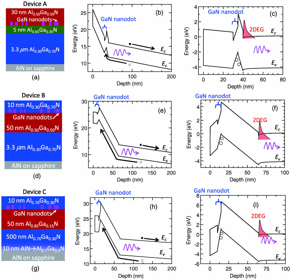
Figure 1.(a) Device A heterostructure and energy band diagram in the pinch-off condition (b) at the onset of illumination and (c) under steady-state illumination. (d) Device B heterostructure and energy band diagram in the pinch-off condition (e) at the onset of illumination and (f) under steady-state illumination. (g) Device C heterostructure and energy band diagram in the pinch-off condition (h) at the onset of illumination and (i) under steady-state illumination.
Figure 1(a) shows the initial design, termed Device A. The channel/spacer is the optically active region, and its bandgap energy () of 4.10 eV (302 nm) is large enough to provide visible-blind detection (). In the off-state, optically generated holes in the channel/spacer drift toward the surface and are captured at the GaN nanodot before reaching the gate electrode. Accumulation of holes at the GaN nanodots causes a large, positive to turn the device on. The GaN nanodots could be placed near the surface or near the channel to maximize [4]. The latter was chosen due to concerns over surface recombination limiting the lifetime of localized holes. However, once the localized holes switch the floating gate HEMT into the on-state, the localized holes and electrons in the channel are in close proximity, which could lead to recombination that quenches the floating gate action and hence the channel. An electron block layer (EBL) was therefore placed between the GaN nanodots and the channel to provide a larger barrier against electron-hole recombination.
While Device A achieved high responsivity, as described in Section 4, examination of its performance prompted a redesign of the heterostructure. Despite the EBL, the proximity between the localized holes and the electrons in the channel likely reduced the dynamic range of the photodetector. In response, the GaN nanodots were moved away from the channel and close to the surface. This HEMT design, termed Device B, is shown in Fig. 1(d). The improved performance of Device B over Device A discounted the initial concern regarding the lifetime of holes captured near the HEMT surface.
A drawback for both Devices A and B was that of the optically active region was too small for solar-blind photodetection. Figure 1(g) shows the third HEMT design used in this study, termed Device C, to achieve solar-blind photodetection. Device C resembles Device B except that the AlN compositions of the AlGaN layers were increased to achieve solar-blind detection.
3. GROWTH, FABRICATION, AND CHARACTERIZATION METHODS
AlGaN HEMTs were grown unintentionally doped by metal organic vapor phase epitaxy (MOVPE) in a Veeco D-125 system at 75 Torr (1 Torr = 133.322 Pa) using and carrier gases and conventional precursors, including trimethylgallium, trimethylaluminum, and ammonia. Figure 1 shows the epitaxial structure of the three types of devices, where the nanodot and barrier layers were each regrown over the channel region. Devices A and B with channels were grown at 1045°C on 3.3 μm thick, unintentionally doped (UID) epilayer grown upon a 1.6 μm thick AlN template grown upon (0001) -plane sapphire substrates misoriented 0.2° toward the -plane. A 5 nm EBL was also grown upon the channel layer for Device A. Device C with an channel was grown at 1045°C by first compositionally grading to from AlN over 10 nm on a 1.4 μm thick AlN template also grown upon (0001) -plane sapphire substrates misoriented 0.2° toward the -plane.
After growth of the channel layer (and EBL layer for Device A), GaN nanodots for all HEMTs were regrown by MOVPE using anodized aluminum oxide growth masks to control the size and density of dots [7]. Growth masks were patterned by first depositing on the AlGaN channel layer using plasma-enhanced chemical vapor deposition (PECVD) followed by the RF magnetron sputter deposition of a low-stress 250 nm thick film of 2 wt. % Nd-doped Al. Using Nd-doped Al prevents the usual surface oxidation upon exposure to air, instead resulting in a smooth and shiny film [8]. As described elsewhere, the films were converted to AAO via electrochemical anodization, forming an array of quasi-hexagonal close packed nanopores. The pores are homogenized and widened to diameters by etching in phosphoric acid [9]. Following AAO patterning, the AAO mask was used as an etch mask to transfer the pore patterns into the using reactive ion etching (RIE). The AAO was then removed using etch to reveal the mask. The epilayer was then reintroduced into the MOVPE reactor for selective area GaN nanodot regrowth at 1045°C. Following GaN nanodot regrowth, the mask was removed using HF.
The GaN nanodots were characterized by atomic force microscopy (AFM). The as-grown GaN nanodot height was too large to use in AlGaN HEMTs because the negative polarization charge at the GaN/AlGaN heterointerface would deplete the underlying HEMT channel. Thus, GaN nanodots were reduced in size using thermal decomposition in the MOVPE reactor at a temperature of 1045°C for 80 min using the same , , and flows used for growth of the AlGaN barrier. Figure 2 shows the AFM image of the nanodots after size reduction. There was a tri-model size distribution of small, medium, and large nanodots. The final GaN nanodot average height was determined by AFM profiling to be , where the standard deviation is indicative of the spread in nanodot size. After the GaN nanodots’ thermal decomposition, the AlGaN barrier region was then grown to finish the heteroepitaxial layer.

Figure 2.AFM image of GaN nanodots after size reduction and prior to AlGaN barrier overgrowth. The image size is .
Circular HEMT devices were fabricated using standard contact photolithography. Devices A and B with channel HEMTs used Ti/Al/Ni/Au deposited via electron beam evaporation for source and drain contracts [10]. Following ohmic metallization, Devices A and B underwent rapid thermal anneal (RTA) at 900°C for 30 s under approximately 1 mTorr of nitrogen. The ohmic contacts were electrically characterized using current-voltage () sweeps of the circular transmission line method structures, and a specific contact resistivity of was determined. Finally, a semitransparent Ni (80 Å, 1 Å = 0.1 nm) gate metal was electron-beam deposited. HEMT devices had a nominal gate length of 1.5 μm, source-to-drain spacing of 10 μm, and a gate width of 660 μm. The gate was equidistant to the source and drain, with gate-to-source and gate-to-drain spacing of 4.25 μm. A similar process was used for Device C with an channel, except that the source and drain contacts consisted of Zr/Al/Mo/Au metals stacks annealed at 1100°C with an estimated [11]. The Zr-based source and drain contacts were found to be more conductive than the Ti-based contacts for the Al-rich barrier but were nonetheless still quite resistive due to the difficulty of achieving ohmic contacts for AlGaN HEMTs with barrier AlN mole fraction .
Optoelectronic responsivity of the HEMTs was measured at 297 K using a Xe arc lamp source filtered through a 0.25-m monochromator with mode-sorting filters to achieve monochromatic illumination in the range –. The optical power of the focused beam from the monochromator was for and for . Photoresponsivity was calculated by dividing by the optical power incident upon the device. Two Keithley 2400 source measurement units with their commons grounded to the source were used to apply gate and drain bias and to measure as a function of time.
4. PHOTODETECTOR EVALUATION
A. Device A: Al0.30Ga0.70N Channel with Nanodots near the Channel
The and data measured in the dark for Device A, shown in Fig. 3 and Fig. 4, respectively, confirm that the GaN nanodots did not adversely affect HEMT characteristics. In the dark, the channel HEMT exhibited , which is comparable with previous reports of the channel HEMT without GaN nanodots [12]. The devices had good pinch-off with with . Sweeping the gate from to and back again revealed no drain current hysteresis in the on-state and only 50 mV of hysteresis in deep subthreshold, which suggests that the GaN nanodots did not cause significant charge trapping in the dark.
Figure 3. data for Device A showing good transistor action with inclusion of GaN nanodots.
Figure 4.Transfer characteristics for Device A in the dark and under UV illumination. The device shows good pinch-off in the dark and switches to an on-state under UV illumination.
The HEMT behavior changed dramatically when illuminated with UV light with optical intensity . Figure 4 shows that, under 4.60 eV illumination, Device A no longer pinches off for up to due to self-biasing by the optically triggered floating gate. The under UV illumination at this intensity is large enough to switch the device from the off-state to the on-state. For example, an electrical bias of in the dark produced a when illuminated. Moreover, increased from 121 mA/mm in the dark to 190 mA/mm under UV illumination. This suggests that the combined electrical bias and potential from the floating gate produces stronger accumulation of sheet charge density in the channel than can be achieved from electrical biasing alone.
Figure 5 shows the optical transient of Device A under 4.70 eV illumination. The shutter opened at time , and increased to 102 mA/mm within 50 ms. After 200 ms of illumination, a 5 ms electrical pulse of , was applied under continuous illumination, which rapidly (less than the 3 ms response time of the current meter) quenched the photocurrent by upon returning to the measurement bias. The mechanism for reset is presumably a recombination of localized holes on GaN nanodots with electrons injected from the gate. When electrical bias was set to 0 V, a persistent and large positive potential from the floating gate caused a strong forward bias on the gate electrode, and the resulting gate current quickly quenched the floating gate. Upon returning to the measurement bias, showed a similar rise time. Upon closing the shutter, a slow decay time in the dark was observed. However, a reset pulse applied in the dark also rapidly quenched the photocurrent by . Thus, despite the slow decay time, the ability to electrically pulse the gate electrode of the phototransistor enables a reset time, either under continuous or modulated illumination, that is much shorter than the rise time. This electrical reset pulse is functionally similar to that used for Geiger-mode APDs and can be useful for low-frequency applications, such as imaging and biodetection, where gate control circuitry can drive the device response without degrading total measurement time below a threshold that is technologically useful. Conversely, technologies such as PMTs and APDs can achieve bandwidth but require higher operational voltage.
Figure 5.Transient response under 4.70 eV illumination and use of an electrical fill pulse to rapidly reset the detector.
The responsivity spectrum for Device A is shown in Fig. 6. Responsivity was measured for with the device electrically biased in the off-state at , . was calculated as the increase in drain current after 40 ms of illumination and a reset pulse used after each transient. This corresponds to a total measurement time (rise time plus reset time) of 45 ms, which is sufficient for low-frequency applications such as UV imaging.
Figure 6.Responsivity spectrum for a 40 ms rise time for Device A at different optical intensities. Inset shows the same data on a linear scale.
The dominant absorption threshold in the responsivity spectrum occurred at 4.00 eV, which corroborates the model of photogenerated holes from the becoming localized on the GaN nanodot as the mechanism for photodetection. Indeed, the 4.00 eV absorption is close to the bandgap energy for the channel and spacer, suggesting that band-to-band absorption in these regions is the main contributor to photodetection. A VRR was observed from the peak ( intensity) compared with the noise floor set by the detection limit of the current meter. The much weaker sub-band gap absorption likely arises from deep level defect absorption that can also increase [13].
The GaN nanodot floating gate HEMTs in this study outperform previously reported visible-blind (Al)GaN HEMT photodetectors that were also electrically biased in the off-state to minimize dark current. channel HEMT photodetectors without GaN nanodots have been examined, where deep level defects act effectively as a spatially distributed floating gate [13]. In that case, a qualitatively similar responsivity spectrum was observed for the nanodot-free HEMT when electrically biased in pinch-off; however, a low was achieved for . The much larger observed for Device A compared with the nanodot-free HEMT demonstrates that the GaN nanodots provide a superior hole localization medium compared with crystal defects. This improvement is due to several reasons. Hole capture on a nanodot is likely easier due to the wider extent of the electrostatic potential well. Further, concentrating localized holes near the gate or channel via nanodots produces a larger [4] than if the holes are randomly distributed on defects across the barrier and/or channel region.
Another type of photodetector used a -type GaN cap on an AlGaN/GaN HEMT to create a depletion region that pinched off the channel immediately below the -type GaN [14,15]. Upon illumination, photogenerated holes in the depletion region acted as a floating gate that accumulated the underlying channel, though no specific means for hole localization was incorporated into the device. Visible-blind range was for [14,15], depending on the absorption threshold. The reasons for larger peak for Device A relative to the GaN HEMTs with a -type gate are the same as listed above, namely, longer hole localization at more favorable locations when using GaN nanodots as an engineered floating gate.
It is worthwhile to compare Device A with other III-nitride visible-blind detectors, such as GaN APDs. Recent studies of visible-blind GaN APDs [16] report gains of operating at in Geiger mode. Gain for an APD is approximately the ratio of current under illumination to the current in the dark. To compare GaN APD and AlGaN photo-HEMT performance, an “effective gain” for AlGaN photo-HEMTs is defined as the ratio of the photocurrent to the dark current. For Device A, this “effective gain” figure is , which is larger than reports for GaN APDs. Additionally, Device A operates at 10 compared with for the GaN APD in Ref. [16], which is a reduction in operation voltage. The greatly improved gain and much reduced operating voltage for the photo-HEMTs compared with APDs demonstrate the utility of developing non-avalanche methods for highly sensitive visible- and solar-blind photodetection.
The dynamic range of Device A was investigated to assess its ability to detect lower power signals. Low level detection is important for UV photodetectors because solid-state UV emitters such as AlGaN-based LEDs have low power compared with visible-emitting LEDs. The optical intensity from the monochromator was attenuated by to using a neutral density filter, and was remeasured under the same bias conditions (Fig. 6). The responsivity spectrum at was qualitatively similar to that at , but the peak increased by for the former. Increasing with reduced intensity occurs, so long as the photon flux remains sufficiently large to overwhelm loss mechanisms that limit the steady-state population of holes localized on the GaN nanodots, such as hole recombination. In such cases, has a relatively small influence on , leading to improved . However, reducing below for Device A resulted in a massive decrease in and a collapse in responsivity. The high minimum threshold required for strong suggests a strong recombination mechanism for holes localized on the GaN nanodots. A likely cause is recombination with electrons in the nearby channel. This recognition prompted a new photodetector design.
B. Device B: Al0.30Ga0.70N Channel with Nanodots near the Surface
Device B used a second HEMT design, shown in Fig. 1(d), to move the GaN nanodots away from the channel and toward the surface to reduce recombination between localized holes and the 2DEG. Reducing the recombination rate between electrons in the channel and holes in the GaN nanodots was expected to increase the dynamic range of the photodetector by reducing the optical generation rate needed to sustain a steady-state population of localized holes large enough to switch the device on.
Figure 7 shows the data measured in the dark and under 4.60 eV illumination for Device B. decreased for Device B relative to Device A, and Device B did not completely pinch-off in the dark. The degraded pinch-off characteristics for Device B are attributed to the quality of the underlying AlGaN template rather than the repositioning of the GaN nanodots because HEMTs without GaN nanodots fabricated from the same wafer showed similar behavior. Nonetheless, Device B exhibited a large photocurrent response, similar to Device A.
Figure 7.Transfer characteristics for Device B in the dark and under UV illumination. Despite the incomplete pinch-off, the device exhibited large .
Figure 8 shows the responsivity spectrum for Device B for a 40 ms rise time under and measured at , using , reset pulses. The qualitative spectral features and the maximum responsivity for Device B are comparable with those of Device A. The VRR for Device B was degraded, however, because the inability to pinch-off in the dark reduced the margin for under illumination.
Figure 8.Responsivity spectrum for a 40 ms rise time for Device B.
The dynamic range of operation for Device B for was investigated by using neutral density filters to reduce . The photoresponse of the detector was measurable for . This significant reduction in minimum optical intensity for detection compared with Device A substantiates the importance of spacing the GaN nanodots away from the channel to minimize hole recombination. Both the magnitude and time constant of the transient varied significantly as functions of , so these values were extracted using a nonlinear least-squares fit of 4.35 eV photocurrent transients to a mono-exponential decay function.
Figure 9 presents these data, showing a rise time equal to the inverse of the extracted time constant and equal to the amplitude of the fitted exponential divided by the incident optical power. The magnitude of decreased by , from 80 mA to 75 μA, compared with a reduction in , resulting in a increase in . A standard two-level model of the carrier capture predicts following the form [17], where is a constant. In this case, increases with decreasing . While the data satisfy this general trend, they deviate from this simple expression. Given that this device does not completely pinch-off, it is likely that is not simply proportional to the trapped carriers at the floating-gate. More detailed modeling of the device characteristics and measurements will be needed to address this effect. The rise time of also decreased with . Interestingly, the ratio of the device gain to the rise time was approximately constant for , suggesting a trade-off similar to the gain-bandwidth product of traditional photodetectors. In this instance, the photo-HEMT gain was defined as the number of electrons collected by the contacts relative to the number of incident photons, i.e., .
Figure 9.Responsivity and bandwidth under 4.35 eV illumination for Device B under different optical intensities.
C. Device C: Al0.70Ga0.30N Channel with Nanodots near the Surface
Devices A and B did not achieve solar-blind detection because the region absorbed most of the incident light. To achieve solar-blind operation, Device C was epitaxially grown and fabricated in a similar manner to Devices A and B, except that the AlN compositions in the channel and barrier regions of the HEMT were increased to 0.70 and 0.85, respectively [Fig. 1(g)]. Figure 10 shows the data measured in the dark and under 5.50 eV illumination for Device C. Good pinch-off characteristics were observed for Device C to demonstrate that placing GaN nanodots near the surface does not necessarily degrade gating action, as was observed for Device B. However, the and therefore were greatly reduced compared with Devices A and B due to highly resistive source and drain contacts (), as is typical for Al-rich AlGaN HEMTs. The thinner channel/spacer absorber region for Device C (500 nm) compared with Devices A and B (3300 nm) also could have limited .
Figure 10.Transfer characteristics for Device C in the dark and under UV illumination.
The responsivity spectrum of Device C is shown in Fig. 11. The optical intensity was with the device electrically biased in the off-state at , with of dark current. was measured for 40 ms, and a reset pulse of , was used. The photodetector signal did not exceed the noise floor for , confirming solar-blind operation. A peak of was attained, achieving an . This SRR compares favorably with metal-semiconductor-metal (MSM) AlGaN heterostructure-based solar-blind detectors [18] and exceeds other AlGaN photo-HEMT results [19,20] and commercial PMTs [1]. The absorption threshold of is less than for the channel/spacer region. The redshift in absorption relative to is attributed to absorption by deep level defect states [13]. Nonetheless, GaN nanodots are still the dominant mechanism for photodetection because this absorption tail accounts for less than 0.1% of the total photoresponse. Reducing the resistivity of the source and drain contacts is expected to be the most important factor to improve for Device C. The sheet resistance for channel and channel HEMTs is similar, which points to the poor contacts of the latter as the primary cause for degraded and hence degraded .
Figure 11.Responsivity for Device C for a 40 ms rise time.
Despite the poor contacts, Device C compares favorably with other solar-blind, AlGaN HEMT-based photodetectors. Yoshikawa et al. [18] demonstrated an AlGaN HEMT with a -type GaN gate for solar-blind detection with a peak illumination with dark current. A metal-semiconductor-metal photodetector formed from an AlGaN HEMT-like structure achieved solar-blind detection with a peak and with a dark current of 100 pA/mm; however, the bandwidth of this photodetector was only 5 Hz [21]. Previous reports of solar-blind photodetection using AlGaN-based HEMTs [13] or metal-semiconductor field effect transistors [20] have achieved higher peak S of and , respectively, by using defects to localize holes. However, these devices were electrically biased in the on-state with large dark currents . Thus, Device C is attractive for its combination of high , low dark current, and sufficient bandwidth for solar-blind imaging applications.
Device C also compares favorably with AlGaN APDs. A recent study of solar-blind AlGaN APDs [22] reported a gain of operating at in Geiger-mode. For comparison, the “effective gain,” as defined in Section 4.A, for Device C is , which is larger than reports for AlGaN APDs. Additionally, Device C operates at 10 compared with for the GaN APD in Ref. [22]. The improved gain and reduced operating voltage for the photo-HEMTs compared with AlGaN APDs demonstrate the potential of photo-HEMTs for solar-blind photodetection.
5. SUMMARY
AlGaN-channel HEMTs were operated as visible- and solar-blind photodetectors by using GaN nanodots as an optically active floating gate. Placing the GaN nanodots near the surface and away from the channel greatly benefited the dynamic range of the floating-gate-HEMTs. The responsivity and temporal response were investigated as a function of optical intensity, achieving responsivity for visible-blind HEMT detector. However, controlling the buffer quality was found to be critical to maintain a low dark current. Solar-blind operation was achieved by tuning the AlN mole fraction of the HEMT channel layer, enabling the same device design to be tuned for either visible- or solar-blind detection. The potential for AlGaN floating-HEMTs to provide large responsivity, moderate bandwidth, and low DC power dissipation makes these devices attractive for applications such as visible- and solar-blind imaging.
Acknowledgment
Acknowledgment. The authors thank J. Barrios and M. Pohl for their device fabrication assistance. The views expressed in the article do not necessarily represent the views of the U.S. Department of Energy or the United States Government.
References
[1] G. A. Shaw, A. M. Siegel, J. Model, A. Geboff, S. Soloviev, A. Vert, P. Sandvik. Deep UV photon-counting detectors and applications. Proc. SPIE, 7320, 732001(2009).
[2] E. J. Gansen, M. A. Rowe, M. B. Greene, D. Rosenberg, T. E. Harvey, M. Y. Su, R. H. Hadfield, S. W. Nam, R. P. Mirin. Operational analysis of a quantum dot optically gated field-effect transistor as a single-photon detector. IEEE J. Sel. Top. Quantum Electron., 13, 967-977(2007).
[3] M. A. Rowe, E. J. Gansen, M. Greene, R. H. Hadfield, T. E. Harvey, M. Y. Su, S. W. Nam, R. P. Mirin, D. Rosenberg. Single-photon detection using a quantum dot optically gated field-effect transistor with high internal quantum efficiency. Appl. Phys. Lett., 89, 253505(2006).
[4] M. A. Rowe, E. J. Gansen, M. B. Greene, D. Rosenberg, T. E. Harvey, M. Y. Su, R. H. Hadfield, S. W. Nam, R. P. Mirin. Designing high electron mobility transistor heterostructures with quantum dots for efficient, number-resolving photon detection. J. Vac. Sci. Technol. B, 26, 1174-1177(2008).
[5] A. J. Shields, M. P. O’sullivan, I. Farrer, D. A. Ritchie, R. A. Hogg, M. L. Leadbeater, C. E. Norman, M. Pepper. Detection of single photons using a field-effect transistor gated by a layer of quantum dots. Appl. Phys. Lett., 76, 3673-3675(2000).
[6] G. Snider. 1D Poisson.
[7] Y. D. Wang, K. Y. Zang, S. J. Chua. Nonlithographic nanopatterning through anodic aluminum oxide template and selective growth of highly ordered GaN nanostructures. J. Appl. Phys., 100, 054306(2006).
[8] C. Rochford, S. J. Limmer, S. W. Howell, T. E. Beechem, M. P. Siegal. Planarized arrays of aligned, untangled multiwall carbon nanotubes with ohmic back contacts. J. Mater. Res., 30, 315-322(2015).
[9] S. J. Limmer, W. G. Yelton, M. P. Siegal, J. L. Lensch-Falk, J. Pillars, D. L. Medlin. Electrochemical deposition of Bi2(Te,Se)3 nanowire arrays on Si. J. Electrochem. Soc., 159, D235-D239(2012).
[10] B. A. Klein, A. G. Baca, A. M. Armstrong, A. A. Allerman, C. A. Sanchez, E. A. Douglas, M. H. Crawford, M. A. Miller, P. G. Kotula, T. R. Fortune, V. M. Abate. Planar ohmic contacts to Al0.45Ga0.55N/Al0.3Ga0.7N high electron mobility transistors. ECS J. Solid State Sci. Technol., 6, S3067-S3071(2017).
[11] A. G. Baca, B. A. Klein, A. A. Allerman, A. M. Armstrong, E. A. Douglas, C. A. Stephenson, T. R. Fortune, R. J. Kaplar. Al0.85Ga0.15N/Al0.70Ga0.30N high electron mobility transistors with Schottky gates and large on/off current ratio over temperature. ECS J. Solid State Sci. Technol., 6, Q161-Q165(2017).
[12] A. G. Baca, A. M. Armstrong, A. A. Allerman, B. A. Klein, E. A. Douglas, C. A. Sanchez, T. R. Fortune. High temperature operation of Al0.45Ga0.55N/Al0.30Ga0.70N high electron mobility transistors. ECS J. Solid State Sci. Technol., 6, S3010-S3013(2017).
[13] A. M. Armstrong, B. Klein, A. A. Allerman, E. A. Douglas, A. G. Baca, M. H. Crawford, G. W. Pickrell, C. A. Sanchez. Visible-blind and solar-blind detection induced by defects in AlGaN high electron mobility transistors. J. Appl. Phys., 123, 114502(2018).
[14] M. Iwaya, S. Miura, T. Fujii, S. Kamiyama, H. Amano, I. Akasaki. High-performance UV detector based on AlGaN/GaN junction heterostructure-field-effect transistor with a p-GaN gate. Phys. Status Solidi C, 6, S972-S975(2009).
[15] M. Ishiguro, K. Ikeda, M. Mizuno, M. Iwaya, T. Takeuchi, S. Kamiyama, I. Akasaki. Control of the detection wavelength in AlGaN/GaN-based hetero-field-effect-transistor photosensors. Jpn. J. Appl. Phys., 52, 08JF02(2013).
[16] P. Suvarna, M. Tungare, J. M. Leathersich, P. Agnihotri, F. Shahedipour-Sandvik, L. D. Bell, S. Nikzad. Design and growth of visible-blind and solar-blind III-N APDs on sapphire substrates. J. Electron. Mater., 42, 854-858(2013).
[17] K. Bergemann, F. Léonard. Room-temperature phototransistor with negative photoresponsivity of 108 A W−1 using fullerene-sensitized aligned carbon nanotubes. Small, 14, 1802806(2018).
[18] A. Yoshikawa, Y. Yamamoto, T. Murase, M. Iwaya, T. Takeuchi, S. Kamiyama, I. Akasaki. High-photosensitivity AlGaN-based UV heterostructure-field-effect-transistor-type photosensors. Jpn. J. Appl. Phys., 55, 05FJ04(2016).
[19] Y. Yamamoto, A. Yoshikawa, T. Kusafuka, T. Okumura, M. Iwaya, T. Takeuchi, S. Kamiyama, I. Akasaki. Realization of high-performance hetero-field-effect-transistor-type ultraviolet photosensors using p-type GaN comprising three-dimensional island crystals. Jpn. J. Appl. Phys., 55, 05FJ07(2016).
[20] S. Muhtadi, S. Hwang, A. Coleman, F. Asif, A. Lunev, M. V. S. Chandrashekhar, A. Khan. Selective area deposited n-Al0.5Ga0.5N channel field effect transistors with high solar-blind ultraviolet photo-responsivity. Appl. Phys. Lett., 110, 171104(2017).
[21] A. Yoshikawa, S. Ushida, K. Nagase, M. Iwaya, T. Takeuchi, S. Kamiyama, I. Akasaki. High-performance solar-blind Al0.6Ga0.4N/Al0.5Ga0.5N MSM type photodetector. Appl. Phys. Lett., 111, 191103(2017).
[22] Z. G. Shao, D. J. Chen, H. Lu, R. Zhang, D. P. Cao, W. J. Luo, Y. D. Zheng, L. Li, Z. H. Li. High-gain AlGaN solar-blind avalanche photodiodes. IEEE Electron Device Lett., 35, 372-374(2014).


