Abstract
We examine the spin-orbit interaction of light and photonic spin Hall effect on the surface of anisotropic two-dimensional atomic crystals. As an example, the photonic spin Hall effect on the surface of black phosphorus is investigated. The photonic spin Hall effect manifests itself as the spin-dependent beam shifts in both transverse and in-plane directions. We demonstrate that the spin-dependent shifts are sensitive to the orientation of the optical axis, doping concentration, and interband transitions. These results can be extensively extended to other anisotropic two-dimensional atomic crystals. By incorporating the quantum weak measurement techniques, the photonic spin Hall effect holds great promise for detecting the parameters of anisotropic two-dimensional atomic crystals.1. INTRODUCTION
Two-dimensional (2D) atomic crystals hold great promise in the application of optoelectronics due to their extraordinary electronic and photonic properties [1,2]. Therefore, a fundamental understanding of the light-matter interaction is essential to optoelectronics applications. The photonic spin Hall effect (SHE) manifesting itself as spin-dependent splitting in the light-matter interaction is considered as a result of the spin-orbit interaction of light [3,4]. The photonic SHE can be regarded as a direct photonic analogy of electronic SHE, which has been extensively studied in 3D bulk crystal [5,6]. The spin-dependent splitting in photonic SHE is generally on subwavelength scales, which can be observed by the signal enhancement technique known as quantum weak measurements [7,8].
More recently, the spin-orbit interaction of light and photonic SHE has been investigated on the surface of 2D atomic crystals. In general, the interpretation of reflection and refraction on the surface of 2D atomically thin crystals is treated as a homogeneous medium with an effective refractive index and an effective thickness. However, it is not necessary to involve the effective refractive index to describe the light-matter interaction [9–11] and spin-orbit interaction [12] on the surface of atomically thin crystals. The quantized Imbert–Fedorov effect and Goos–Hänchen effect have been theoretically predicted in the quantum Hall regime of graphene-substrate systems [13,14]. Photonic Hall shifts are sensitive to spin-and-valley properties of the charge carriers, providing an unprecedented pathway to investigate spintronics and valleytronics [15]. The beam shifts on the surface of graphene have been observed via weak measurements [16,17]. In addition, the strong spin-orbit interaction and giant spin-dependent shifts on the surface of graphene have also been predicted [18,19].
Anisotropic 2D atomic crystals provide an extra degree of freedom to tailor the light-matter interaction due to the strong anisotropy [20]. Motivated by the interesting properties, we attempt to examine the spin-orbit interaction of light and photonic SHE on the surface of anisotropic 2D atomic crystals. Black phosphorus, an elemental layered material composed of layers of atoms, has an atomic structure that resembles graphene. But the atomic rings in black-phosphorus layers exhibit a puckered structure, which makes it have strong anisotropic properties [21]. In this paper, a general model is developed to describe the photonic SHE in reflection on the surface of anisotropic 2D atomic crystals. Based on this model, both transverse and in-plane spin-dependent splitting in photonic SHE can be obtained. We demonstrate that the spin-dependent shifts are sensitive to the orientation of the optical axis, doping concentration, and interband transitions.
Sign up for Photonics Research TOC. Get the latest issue of Photonics Research delivered right to you!Sign up now
2. GENERAL THEORETICAL MODEL
We first establish a general model to describe the photonic SHE on the anisotropic atomic crystals. This model can be extensively extended to other 2D anisotropic atomic crystals. Let us consider a Gaussian wave packet with monochromatic frequency impinging from air to the surface of anisotropic 2D atomic crystals (Fig. 1). The axis of the laboratory Cartesian frame () is normal to the surface. A black phosphorus sheet is placed on top of substrate. In addition, we use the coordinate frames () and () to denote the central wave vectors of incidence and reflection, respectively.
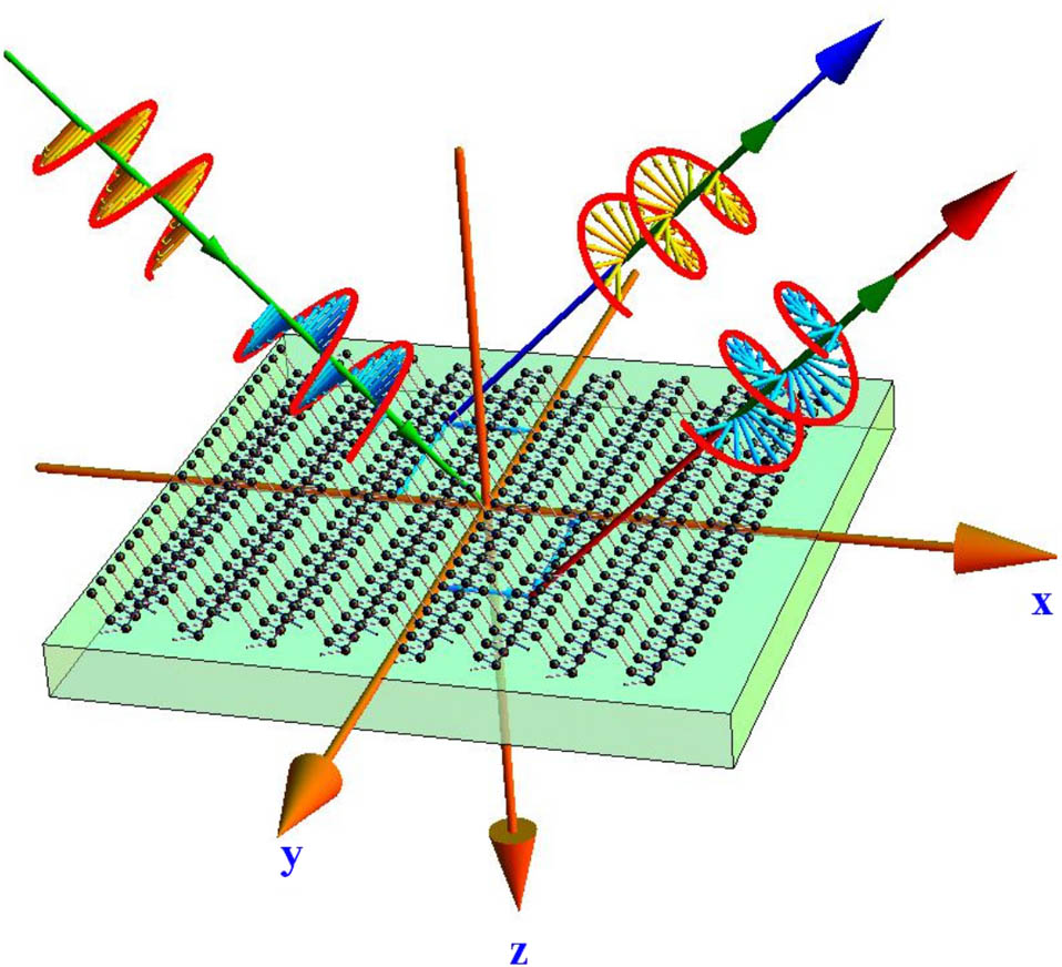
Figure 1.Schematic illustration of the wave reflection at a surface of black phosphorus in a Cartesian coordinate system. A black phosphorus sheet is placed on the top of a homogeneous and isotropic substrate. The photonic SHE occurs on the reflecting surface and exhibits in-plane and transverse spin Hall shifts.
As a strong anisotropic 2D atomic crystal, black phosphorus has the conductivity tensor, which accounts for both the intraband electron motions and the interband electron transitions: . Here, is the concentration of electrons, represents relaxation time, and represents the effective mass of electrons along the direction; represents the different strength of the interband component, and is the frequency of the onset of interband transitions for the component of the conductivity [22]. We write the conductivity as the matrix form: where and denote the transverse and longitudinal conductivities of black phosphorus, respectively. In general, when the incident plane and the orientation of the crystal axis are not coincident, the diagonal elements of the conductance matrix are nonzero. The conductance matrix can be computed as
Here, and are coordinate transformation matrices: where is the optical axis angle. From Eq. (3), the matrix elements of conductivity can be rewritten as
Here, , , and denote the transverse, longitudinal, and crossed conductivity, respectively.
We now consider how conductivity changes with the frequency, as shown in Figs. 2(a)–2(d). In general, two distinct regimes in the electromagnetic response of the anisotropic 2D material can be identified. If the frequency is sufficiently low, the conductivity is of a pure Drude type. The anisotropic properties are attributed to the effective mass of electrons in different directions. If the frequency is sufficiently high, the contribution from interband electron transitions may become dominant, and the imaginary part of the conductivity becomes negative. When the optical axis angle is chosen as , the conductivity exhibits strong anisotropic properties and the crossed competent is absent [Figs. 2(a) and 2(b)]. When the optical axis angle is chosen as , both the transverse and the longitudinal conductivities are modulated; meanwhile, the crossed conductivity appears [Figs. 2(c) and 2(d)].

Figure 2.Real and imaginary parts of the conductivity of the 2D atomic crystal as a function of frequency. Parameters are set as , , and . The frequency of interband electron transitions is present at . (a), (b) The optical axis is chosen as . (c), (d) The optical axis is chosen as . The doping concentration of the 2D atomic crystal is .
For certain frequency and doping concentrations, the components of conductivity can be modulated by the optical axis angle (Fig. 3). The crossed conductivity when the optical axis chosen is or [Figs. 3(a) and 3(b)]. For a certain frequency and a certain optical axis angle, we find that both the real and the imaginary parts of conductivity components linearly increase as the concentration increases [Figs. 3(c) and 3(d)]. Therefore, the anisotropic properties of the 2D atomic crystal can be effectively enhanced by increasing the doping concentration. More importantly, the crossed conductivity can be modulated by the optical axis. The crossed conductivity will play an important role in spin-orbit interaction of light and will lead to the in-plane spin Hall shifts.
Figure 3.(a) Real and (b) imaginary parts of the conductivity of the 2D atomic crystal as a function of optical axis angles. The parameters of the 2D atomic crystal are and . (c) Real and (d) imaginary parts of the conductivity as a function of doping concentration. The optical axis is chosen as . Other parameters are the same as in Fig. 2.
3. PHOTONIC SHE
To examine the light-matter interaction on the surface of the anisotropic 2D atomic crystal, we need to obtain the Fresnel’s coefficients from the boundary conditions. The reflected and transmitted amplitudes satisfy the following equations:
Here, is the incidence angle, and is the refraction angle. is the impedance in air, and is the impedance in media. And in general, . In this case, the Fresnel’s coefficients are obtained as
Here, , , , , , and , where is the refraction angle. , are permittivity and permeability in vacuum; is the permittivity of the substrate. The occurrence of crossed conductivity and is attributed to the emergence of and . When or , we get , which leads to .
For horizontal polarization () and vertical polarization (), the corresponding individual wave-vector components can be expressed by and : where and are the incident and reflected wave vectors, respectively. After reflection, and evolve as , where
We then obtain where is the wave vector in vacuum. To accurately describe the photonic SHE, Fresnel reflection coefficients are confined to the first order in a Taylor series expansion. The polarizations associated with the angular spectrum components experience different rotations in order to satisfy the boundary condition after reflection.
The photonic SHE manifests itself as spin-dependent splitting, which appears in-plane and in transverse directions. To reveal the photonic SHE of light, we now determine the in-plane and transverse shifts of the wave packet. In the spin basis set, the polarization of and can be decomposed into two orthogonal spin components: where and represent the left- and right-circular polarization components, respectively.
We assume that the wave function in momentum space of the incident wave packet can be specified by the following expression: where is the width of wave function. Then the total wave function is made up of the packet spatial extent and the polarization description. From Eqs. (19), (20), and (23), the reflected wave function can be written as
Here, the boundary conditions and , as well as the approximations of are introduced. In addition, the spin-independent terms have been neglected, and only the spin-dependent ones are retained. The in-plane spin Hall shifts can be written as
The transverse spin Hall shifts can be obtained as
Note that the spin Hall shifts are complex and can be written as . Here, the real part is related to the spin Hall shift in the position space, while the imaginary part is associated with the spin Hall shifts in the momentum space [23,24].
The photonic SHE is considered as a result of the spin-orbit interaction of light. The origin of these spin-orbit interaction terms and in Eqs. (24) and (25) lies in the transverse nature of the photon polarization, and the polarizations associated with the plane-wave components experience different rotations in order to satisfy the transversality after reflection, hence inducing spin-dependent geometric phases and [25]. In general, the in-plane geometric phase () is absent on the surface of conventional 3D crystals. In this case, however, the crossed conductivity plays an important role in the spin-orbit interaction of light. Moreover, the crossed conductivity can be modulated by the optical axis angle. Therefore, the spin-orbit interaction of light on the surface of an anisotropic 2D atomic crystal can also be modulated and the in-plane geometric phase arises.
The in-plane spin Hall shifts of the wave packet at initial position () are given by
Substituting Eqs. (24) and (25) into Eq. (30), the in-plane spin Hall shifts of the two spin components can be written as
The transverse spin Hall shifts of the two spin components can be written as
Substituting Eqs. (24) and (25) into Eq. (33), respectively, we obtain the transverse spin Hall shifts for two spin components:
To reveal the relation between the photonic SHE and the parameters of anisotropic 2D atomic crystals, we plot the spin Hall shifts as a function of the frequency and the optical axis angle (Fig. 4). It has been shown that the conductivity presents a transition at the frequency of , which is the frequency of the onset of interband transitions (Fig. 2). Accordingly, the spin Hall shifts exhibit transition points at this frequency. Both the in-plane and transverse spin Hall shifts exhibit a large value (at the wavelength level) [Figs. 4(a) and 4(b)], since the incident angle is chosen as 60°, which is near the Brewster angle. This interesting phenomenon is similar to the spin Hall shift on the surface of conventional 3D crystals [26]. For different optical angles, the spin Hall shifts are significantly different due to the strong anisotropic properties of the 2D atomic crystal. We note that the in-plane spin Hall shifts and crossed conductivity have a similar change tendency with the optical axis. While the transverse spin Hall shifts and the transverse (or longitudinal) conductivity exhibit a similar tendency, it is demonstrated that the spin Hall shifts are sensitive to the variance of the frequency and the optical axis angle.
Figure 4.(a) In-plane and (b) transverse spin-dependent shifts on the surface of anisotropic 2D atomic crystal as a function of optical axis angle and frequency. The incident light impinges on the substrate at , the refractive index of the substrate is assumed as 2, and the doping concentration is .
We next plot the spin Hall shifts as a function of the optical axis angle and doping concentration, as shown in Figs. 5(a) and 5(b). It has been shown that the conductivities increase linearly with the doping concentration [Figs. 3(c) and 3(d)]. We find that the spin Hall shifts have a similar variation tendency with the real and imaginary parts of the conductivities. When or , the longitudinal spin Hall shifts are zero. This phenomenon can be explained from Eqs. (31) and (32), since leads to , and only the transverse geometric phase arises. In addition, the conductivity will be enhanced by increasing the doping concentration and thereby change the Brewster angle [27]. It has been demonstrated that the large spin Hall shifts can be obtained due to the strong spin-orbit interaction [28]. As a result, the spin Hall shifts are sensitive to the change of the doping concentration. Therefore, the photonic SHE offers a convenient way to determine the doping concentration and optical axis angle by a direct optical measurement.
Figure 5.(a) In-plane and (b) transverse spin Hall shifts on the anisotropic 2D atomic crystal as a function of the optical axis angle and doping concentration. The frequency . Other parameters are the same as in Fig. 4.
In our theoretical model, only single black phosphorus layer is considered. It would be interesting to consider the effect of increasing the number of black phosphorus layers, as it is known that this results in modifying the bandgap of the material [29]. As a result, the optical absorption spectra and conductivity are changed. In addition, the preferred conducting direction can be rotated with the appropriate biaxial or uniaxial strain [30]. This will be useful for exploring unusual quantum Hall effects and exotic electronic and mechanical applications based on black phosphorus. In our case, we have shown that the spin Hall shifts are sensitive to the change of the conductivity. Therefore, increasing the number of black phosphorus layers or anisotropic strain would certainly impact the photonic SHE and provide an extra degree of control of the spin Hall shifts.
Weak measurement [7] is an important and convenient approach for detecting the beam shifts. In the procedure of weak measurements, the quantum system is first preselected as an initial state. Then the observable is very weakly coupled to the pointer state. Finally, the pointer position is recorded when the quantum system is postselected at a final state. When the fidelity between the pre- and post-selections is small, the weak value can be very large, indicating a large position shift of the probe [31]. By incorporating quantum weak measurement techniques, the photonic SHE holds great promise for detecting the parameters of anisotropic 2D atomic crystals. In addition, the enhanced SHE should be able to be obtained, due to the tunable conductivity and surface plasmon resonance [32].
4. CONCLUSION
In conclusion, we have revealed the photonic SHE on the surface of an anisotropic 2D atomic crystal. The photonic SHE manifests itself as in-plane and transverse spin-dependent splitting due to the spin-orbit interaction of light. As an example, the spin Hall shifts on the surface of black phosphorus have been investigated. We have demonstrated that the spin Hall shifts are sensitive to the orientation of the optical axis, doping concentration, and interband transitions. By incorporating quantum weak measurement techniques, the photonic SHE holds great promise for detecting the parameters of anisotropic 2D atomic crystals. We believe that these results can be extensively extended to other anisotropic 2D atomic crystals.
References
[1] A. K. Geim, K. S. Novoselov. The rise of graphene. Nat. Mater., 6, 183-191(2007).
[2] F. Bonaccorso, Z. Sun, T. Hasan, A. C. Ferrari. Graphene photonics and optoelectronics. Nat. Photonics, 4, 611-622(2010).
[3] M. Onoda, S. Murakami, N. Nagaosa. Hall effect of light. Phys. Rev. Lett., 93, 083901(2004).
[4] K. Y. Bliokh, Y. P. Bliokh. Conservation of angular momentum, transverse shift, and spin Hall effect in reflection and refraction of an electromagnetic wave packet. Phys. Rev. Lett., 96, 073903(2006).
[5] K. Y. Bliokh, F. J. Rodríguez-Fortuño, F. Nori, A. V. Zayats. Spin-orbit interactions of light. Nat. Photonics, 9, 796-808(2015).
[6] X. Ling, X. Zhou, K. Huang, Y. Liu, C. W. Qiu, H. Luo, S. Wen. Recent advances in the spin Hall effect of light. Rep. Prog. Phys., 80, 066401(2017).
[7] Y. Aharonov, D. Z. Albert, L. Vaidman. How the result of a measurement of a component of the spin of a spin-1/2 particle can turn out to be 100. Phys. Rev. Lett., 60, 1351-1354(1988).
[8] O. Hosten, P. Kwiat. Observation of the spin Hall effect of light via weak measurements. Science, 319, 787-790(2008).
[9] M. Merano. Fresnel coefficients of a two-dimensional atomic crystal. Phys. Rev. A, 93, 013832(2016).
[10] M. Merano. Transverse electric surface mode in atomically thin boron-nitride. Opt. Lett., 41, 2668-2671(2016).
[11] M. Merano. Optical beam shifts in graphene and single-layer boron-nitride. Opt. Lett., 41, 5780-5783(2016).
[12] L. Cai, M. Liu, S. Chen, Y. Liu, W. Shu, H. Luo, S. Wen. Quantized photonic spin Hall effect in graphene. Phys. Rev. A, 95, 013809(2017).
[13] W. J. M. Kort-Kamp, N. A. Sinitsyn, D. A. R. Dalvit. Quantized beam shifts in graphene. Phys. Rev. B, 93, 081410(2016).
[14] W. Wu, S. Chen, C. Mi, W. Zhang, H. Luo, S. Wen. Giant quantized Goos–Hänchen effect on the surface of graphene in the quantum Hall regime. Phys. Rev. A, 96, 043814(2017).
[15] W. J. M. Kort-Kamp. Topological phase transitions in the photonic spin Hall effect. Phys. Rev. Lett., 119, 147401(2017).
[16] X. Zhou, X. Li, H. Luo, S. Wen. Identifying graphene layers via spin Hall effect of light. Appl. Phys. Lett., 101, 251602(2012).
[17] S. Chen, C. Mi, L. Cai, M. Liu, H. Luo, S. Wen. Observation of the Goos–Hänchen shift in graphene via weak measurements. Appl. Phys. Lett., 110, 031105(2017).
[18] M. Liu, L. Cai, S. Chen, Y. Liu, H. Luo, S. Wen. Strong spin-orbit interaction of light on the surface of atomically thin crystals. Phys. Rev. A, 95, 063827(2017).
[19] W. Zhu, M. Jiang, H. Guan, J. Yu, H. Lu, J. Zhang, Z. Chen. Tunable spin splitting of Laguerre-Gaussian beams in graphene metamaterials. Photon. Res., 5, 684-688(2017).
[20] F. Xia, H. Wang, Y. Jia. Rediscovering black phosphorus as an anisotropic layered material for optoelectronics and electronics. Nat. Commun., 5, 4458(2014).
[21] T. Low, R. Roldán, H. Wang, F. Xia, P. Avouris, L. M. Moreno, F. Guinea. Plasmons and screening in monolayer and multilayer black phosphorus. Phys. Rev. Lett., 113, 106802(2014).
[22] A. Nemilentsau, T. Low, G. Hanson. Anisotropic 2D materials for tunable hyperbolic plasmonics. Phys. Rev. Lett., 116, 066804(2016).
[23] X. Ling, X. Zhou, X. Yi, W. Shu, Y. Liu, S. Chen, H. Luo, S. Wen, D. Fan. Giant photonic spin Hall effect in momentum space in a structured metamaterial with spatially varying birefringence. Light Sci. Appl., 4, e290(2015).
[24] C. Mi, S. Chen, X. Zhou, K. Tian, H. Luo, S. Wen. Observation of tiny polarization rotation rate in total internal reflection via weak measurements. Photon. Res., 5, 92-96(2017).
[25] M. V. Berry. Quantal phase factors accompanying adiabatic changes. Proc. R. Soc. London Ser. A, 392, 45-57(1984).
[26] H. Luo, X. Zhou, W. Shu, S. Wen, D. Fan. Enhanced and switchable spin Hall effect of light near the Brewster angle on reflection. Phys. Rev. A, 84, 043806(2011).
[27] C. Mi, S. Chen, W. Wu, W. Zhang, X. Zhou, X. Ling, W. Shu, H. Luo, S. Wen. Precise identification of graphene layers at the air-prism interface via a pseudo-Brewster angle. Opt. Lett., 42, 4135-4138(2017).
[28] X. Zhou, Z. Xiao, H. Luo, S. Wen. Experimental observation of the spin Hall effect of light on a nanometal film via weak measurements. Phys. Rev. A, 85, 043809(2012).
[29] V. Tran, R. Soklaski, Y. Liang, L. Yang. Layer-controlled band gap and anisotropic excitons in few-layer black phosphorus. Phys. Rev. B, 89, 235319(2014).
[30] L. Fei, L. Yang. Strain-engineering the anisotropic electrical conductance of few-layer black phosphorus. Nano Lett., 14, 2884-2889(2014).
[31] J. Dressel, M. Malik, F. M. Miatto, A. N. Jordan, R. W. Boyd. Colloquium: understanding quantum weak values: basics and applications. Rev. Mod. Phys., 86, 307-316(2014).
[32] Y. Xiang, X. Jiang, Q. You, J. Guo, X. Dai. Enhanced spin Hall effect of reflected light with guided-wave surface plasmon resonance. Photon. Res., 5, 467-472(2017).


