• Photonics Research
  • Vol. 10, Issue 12, 2901 (2022)
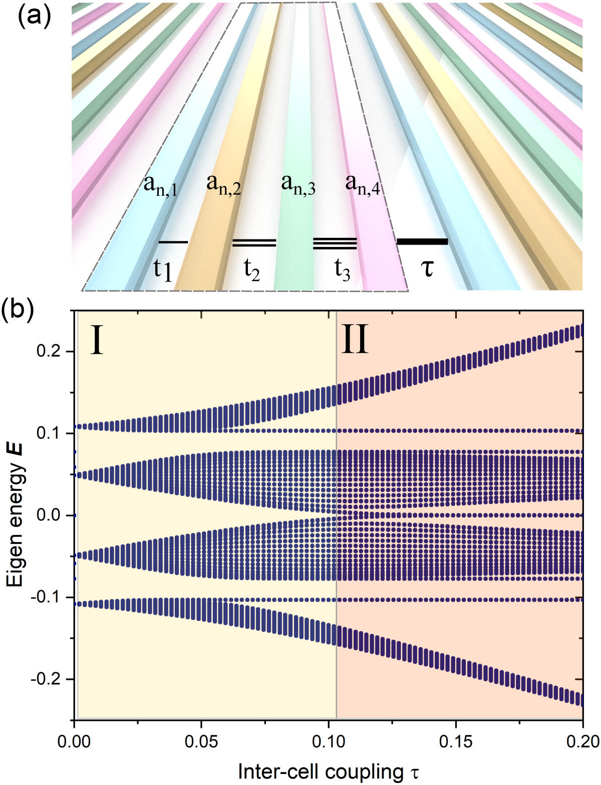
Ze-Sheng Xu1, Jun Gao1、2、*, Govind Krishna1, Stephan Steinhauer1, Val Zwiller1, and Ali W. Elshaari1、3、*
Author Affiliations
  • 1Department of Applied Physics, Royal Institute of Technology, Albanova University Centre, 106 91 Stockholm, Sweden
  • 2e-mail:
  • 3e-mail:
  • show less
    DOI: 10.1364/PRJ.474165 Cite this Article Set citation alerts
    Ze-Sheng Xu, Jun Gao, Govind Krishna, Stephan Steinhauer, Val Zwiller, Ali W. Elshaari. Direct measurement of topological invariants in photonic superlattices[J]. Photonics Research, 2022, 10(12): 2901 Copy Citation Text show less
    (a) Schematic of an SSH4 superlattice. The lattice consists of four sites per unit cell, with intracell coupling amplitudes t1−3 and intercell coupling amplitude τ. (b) Energy spectrum at different intercell coupling amplitude τ. The intracell coupling amplitudes are fixed at t1=0.0587, t2=0.0503, and t3=0.0902. As the intercell coupling amplitude is increased, the first and third bandgaps never close. The situation is different for the bandgap centered at zero energy, where we can see the closure and reopening of the bandgap at τ0=t1t3/t2 together with the appearance of energy-degenerate right and left edge localized topologically protected states. Two regions are highlighted I and II, which correspond to the topologically trivial and nontrivial bandgap number N2, respectively.
    Fig. 1. (a) Schematic of an SSH4 superlattice. The lattice consists of four sites per unit cell, with intracell coupling amplitudes t13 and intercell coupling amplitude τ. (b) Energy spectrum at different intercell coupling amplitude τ. The intracell coupling amplitudes are fixed at t1=0.0587, t2=0.0503, and t3=0.0902. As the intercell coupling amplitude is increased, the first and third bandgaps never close. The situation is different for the bandgap centered at zero energy, where we can see the closure and reopening of the bandgap at τ0=t1t3/t2 together with the appearance of energy-degenerate right and left edge localized topologically protected states. Two regions are highlighted I and II, which correspond to the topologically trivial and nontrivial bandgap number N2, respectively.
    (a), (b) Simulated light evolution pattern in superlattices. The two superlattices have the same parameters as in Fig. 1(a) band diagram, with τ1=0.052 (<τ0) in (a) and τ2=0.194 (>τ0) in (b), corresponding to topologically trivial and nontrivial phases, respectively. Bulk excitation is used at the eighth cell a8=(1/2)(1,0,1,0). (c) Beam displacement calculation of trivial superlattice (gold) and nontrivial superlattice (brown). The numerical calculation involves summing over all the superlattice cells at different propagation distances using Eq. (3). Two quantized values of 0 and −0.25 are found in the case of trivial and nontrivial superlattices. (d) Phase difference versus beam displacement. The beam displacement (dotted lines, left y axis) is calculated for different phases θ between the two input waveguides an(0)=(1/2)(1,0,eiθ1,0), for the trivial phase (gold) and the nontrivial lattice (brown). The difference between the two beam displacements in the trivial and nontrivial superlattices is shown by the green solid line (right side y axis) with robustness.
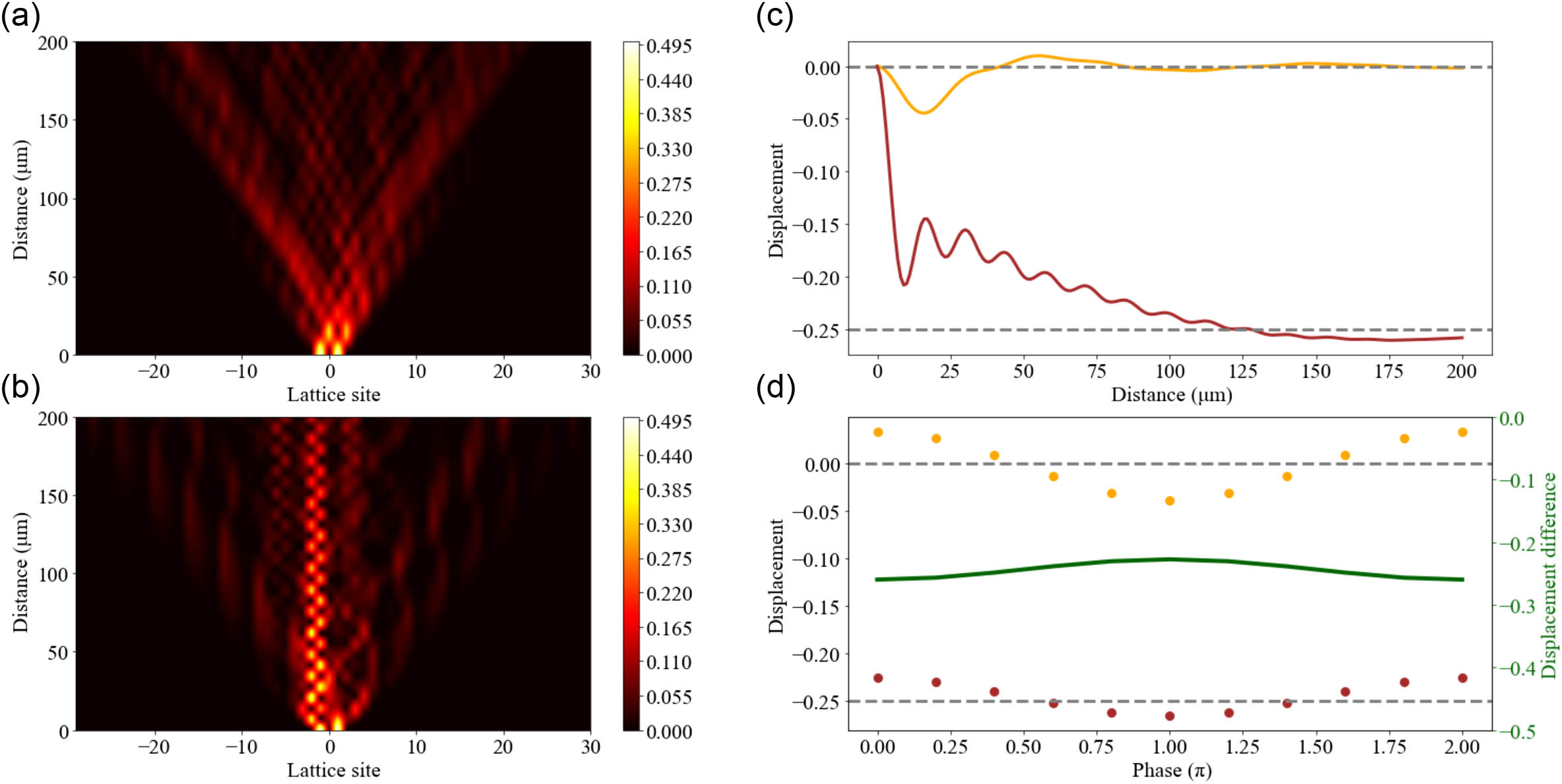
    Fig. 2. (a), (b) Simulated light evolution pattern in superlattices. The two superlattices have the same parameters as in Fig. 1(a) band diagram, with τ1=0.052 (<τ0) in (a) and τ2=0.194 (>τ0) in (b), corresponding to topologically trivial and nontrivial phases, respectively. Bulk excitation is used at the eighth cell a8=(1/2)(1,0,1,0). (c) Beam displacement calculation of trivial superlattice (gold) and nontrivial superlattice (brown). The numerical calculation involves summing over all the superlattice cells at different propagation distances using Eq. (3). Two quantized values of 0 and −0.25 are found in the case of trivial and nontrivial superlattices. (d) Phase difference versus beam displacement. The beam displacement (dotted lines, left y axis) is calculated for different phases θ between the two input waveguides an(0)=(1/2)(1,0,eiθ1,0), for the trivial phase (gold) and the nontrivial lattice (brown). The difference between the two beam displacements in the trivial and nontrivial superlattices is shown by the green solid line (right side y axis) with robustness.
    Schematic of the experimental setup. A 795 nm CW laser is used to excite the chip via a lensed fiber, and the TE mode of the waveguide is selected with a polarization controller. To confirm the excited mode polarization in the superlattice, the chip’s output is free-space-coupled to an optical power meter after a polarizing beam splitter. A microscope equipped with a CCD camera is used to top-image the light dispersed from the superlattice. To measure the light dynamics in the SSH4 photonic lattice, nanoscattering structures are introduced to the odd and even cells in the lattice [34], separated by a distance of 5 μm. The inset shows the top image of the lattice, where the top and bottom rows sample the light propagating in the odd and even cells, respectively. In total, the device has a length of 300 μm, with five sampling sections measured at distances of 40, 80, 120, 160, and 200 μm. (b) False colored SEM image of integrated photonic chip. The input waveguide branches to the SSH4 superlattice (yellow) and the reference port (green). A 50:50 Y-shaped beam splitter (blue) is used to excite the superlattice in the a8=(1/2)(1,0,1,0) state. (c) Magnified SEM image of the nanoscattering structures at the odd and even cells to sample the light intensity in the superlattice. The dotted white boxes indicate the location of the nanoscattering structure. The scale bars in (b) and (c) correspond to lengths of 40 μm and 2 μm, respectively.
    Fig. 3. Schematic of the experimental setup. A 795 nm CW laser is used to excite the chip via a lensed fiber, and the TE mode of the waveguide is selected with a polarization controller. To confirm the excited mode polarization in the superlattice, the chip’s output is free-space-coupled to an optical power meter after a polarizing beam splitter. A microscope equipped with a CCD camera is used to top-image the light dispersed from the superlattice. To measure the light dynamics in the SSH4 photonic lattice, nanoscattering structures are introduced to the odd and even cells in the lattice [34], separated by a distance of 5 μm. The inset shows the top image of the lattice, where the top and bottom rows sample the light propagating in the odd and even cells, respectively. In total, the device has a length of 300 μm, with five sampling sections measured at distances of 40, 80, 120, 160, and 200 μm. (b) False colored SEM image of integrated photonic chip. The input waveguide branches to the SSH4 superlattice (yellow) and the reference port (green). A 50:50 Y-shaped beam splitter (blue) is used to excite the superlattice in the a8=(1/2)(1,0,1,0) state. (c) Magnified SEM image of the nanoscattering structures at the odd and even cells to sample the light intensity in the superlattice. The dotted white boxes indicate the location of the nanoscattering structure. The scale bars in (b) and (c) correspond to lengths of 40 μm and 2 μm, respectively.
    (a), (b) Light intensity over different cells in topologically trivial and nontrivial superlattices, respectively. The experimental data are shown by the dotted lines, while the solid lines represent the numerically modeled superlattice. The coupling amplitudes in the simulated Hamiltonian are directly determined from the chip physical dimensions and refractive indices of different materials; no free fitting parameters are utilized. As the propagation distance increases, the trivial superlattice has greater spread around the input eighth cell. (c) Experimentally measured beam displacement. Measured topological invariant of the trivial superlattice (gold) and nontrivial superlattice (brow) at different propagation distances. The beam displacement is evaluated through integrating the intensity multiplied by the cell numbers over the cell numbers in Eq. (3). In the case of the trivial photonic superlattices, we measure a beam displacement of 0.088, while in the case of nontrivial photonic superlattices, −0.245. The results show good agreement with the theoretical values (dotted lines) of 0 and −0.25. A distinct gap can be observed for the different topological phases.
    Fig. 4. (a), (b) Light intensity over different cells in topologically trivial and nontrivial superlattices, respectively. The experimental data are shown by the dotted lines, while the solid lines represent the numerically modeled superlattice. The coupling amplitudes in the simulated Hamiltonian are directly determined from the chip physical dimensions and refractive indices of different materials; no free fitting parameters are utilized. As the propagation distance increases, the trivial superlattice has greater spread around the input eighth cell. (c) Experimentally measured beam displacement. Measured topological invariant of the trivial superlattice (gold) and nontrivial superlattice (brow) at different propagation distances. The beam displacement is evaluated through integrating the intensity multiplied by the cell numbers over the cell numbers in Eq. (3). In the case of the trivial photonic superlattices, we measure a beam displacement of 0.088, while in the case of nontrivial photonic superlattices, 0.245. The results show good agreement with the theoretical values (dotted lines) of 0 and 0.25. A distinct gap can be observed for the different topological phases.
    Refractive indices measured by ellipsometry. The measurement is performed for wavelengths between 700 nm and 1000 nm, at 5 nm steps. The blue curve shows the refractive index of Si3N4, while the green curve shows the refractive index of the SiO2 cladding. The operating wavelength of the device is highlighted at 795 nm.
    Fig. 5. Refractive indices measured by ellipsometry. The measurement is performed for wavelengths between 700 nm and 1000 nm, at 5 nm steps. The blue curve shows the refractive index of Si3N4, while the green curve shows the refractive index of the SiO2 cladding. The operating wavelength of the device is highlighted at 795 nm.
    Coupling strength between the waveguides. (a) and (b) show the real x component of the electric field for the odd and even TE modes supported in a waveguide dimer. (c) Coupling strength per micrometer between two waveguides for different gaps. The simulated data are fitted according to Eq. (A1) with a decay constant a of 0.0078 μm−1.
    Fig. 6. Coupling strength between the waveguides. (a) and (b) show the real x component of the electric field for the odd and even TE modes supported in a waveguide dimer. (c) Coupling strength per micrometer between two waveguides for different gaps. The simulated data are fitted according to Eq. (A1) with a decay constant a of 0.0078  μm1.
    Ze-Sheng Xu, Jun Gao, Govind Krishna, Stephan Steinhauer, Val Zwiller, Ali W. Elshaari. Direct measurement of topological invariants in photonic superlattices[J]. Photonics Research, 2022, 10(12): 2901
    Download Citation