Ze-Sheng Xu, Jun Gao, Govind Krishna, Stephan Steinhauer, Val Zwiller, Ali W. Elshaari, "Direct measurement of topological invariants in photonic superlattices," Photonics Res. 10, 2901 (2022)
Copy Citation Text
Since the discovery of topological insulators, topological phases have generated considerable attention across the physics community. The superlattices in particular offer a rich system with several degrees of freedom to explore a variety of topological characteristics and control the localization of states. Albeit their importance, characterizing topological invariants in superlattices consisting of a multi-band structure is challenging beyond the basic case of two-bands as in the Su–Schreifer–Heeger model. Here, we experimentally demonstrate the direct measurement of the topological character of chiral superlattices with broken inversion symmetry. Using a CMOS-compatible nanophotonic chip, we probe the state evolving in the system along the propagation direction using novel nanoscattering structures. We employ a two-waveguide bulk excitation scheme to the superlattice, enabling the identification of topological zero-energy modes through measuring the beam displacement. Our measurements reveal quantized beam displacement corresponding to 0.088 and -0.245, in the cases of trivial and nontrivial photonic superlattices, respectively, showing good agreement with the theoretical values of 0 and -0.25. Our results provide direct identification of the quantized topological numbers in superlattices using a single-shot approach, paving the way for direct measurements of topological invariants in complex photonic structures using tailored excitations with Wannier functions.
1. INTRODUCTION
Since the discovery of superlattices in 1925 by Johansson and Linde [1] in X-ray diffraction experiments, there has been a tremendous interest in their properties in the fields of optics and condensed matter physics [2–5], which led to the realization of key enabling technologies such as the quantum cascade lasers [6]. The topology of the band structure is particularly important. It provides new means of controlling light propagation and simulating topological phases of matter in optics [7–12]. Furthermore, edge states in topological lattices exhibit resistance to disorder as they are protected from backscattering on the band structure level [13,14].
A 1D lattice of dimers, famously labeled the Su–Schrieffer–Heeger (SSH) model [15], or specifically referring to the two lattice sites per unit cell, provides the simplest system with topologically trivial and nontrivial edge states [16], and has been widely studied in different physical platforms [17–21]. From a topology perspective, higher-order superlattices , with sites per unit cell [22–24], enable a larger parameter space with multi-band structure for photonic state engineering. The model shows richer physics with the simultaneous existence of topologically trivial and nontrivial states. Meanwhile, directly probing the Zak phase in photonic lattice enables designing the system parameters to tune the number of topologically protected states, paving the way for topologically protected and robust mode-division multiplexing in photonic networks through manipulating the coupling strengths between waveguides. In a series of experiments, topological invariants have been probed through several techniques such as Bloch oscillations [25] and quantum walks [26–30]. However, a larger number of bands can limit the use of imaging techniques to identify protected edge localized states, as topological and nontopological states can coexist in different bands [22]. The probing of such a multi-band structure has proved to be challenging beyond the dimer case. A more general approach would be to infer the Zak phase of a particular band through using the beam displacement approach, with Wannier function input. Although this measurement scheme is general and can be applied to a superlattice with arbitrary number of sites in the unit cell, the Wannier function excitation technique is difficult to implement experimentally, requiring precise control of the field amplitudes and phases in each individual lattice site.
2. CHIRAL SUPERLATTICES WITH BROKEN INVERSION SYMMETRY
We experimentally simplify the Wannier function excitation and realize direct measurement of the topological character in an engineered chiral system with broken inversion symmetry [22]. The schematic of the designed system is shown in Fig. 1(a). It consists of a superlattice with four waveguides per unit cell with equal on-site potential. The Hamiltonian is presented in Eq. (1), with only nearest neighbor coupling between lattice sites: are the creation and annihilation operators at cell and lattice site . and are the coupling amplitudes between lattice sites within each cell and between different cells, respectively. The topological character of the band structure is directly related to the Zak phase of the band. The Zak phase is calculated by integrating the Berry connection along the wave vector axis in the Brillouin zone. We employ to represent the bandgaps in a system. Our superlattice model shown in Fig. 1(a) contains bandgaps. The topology of the th bandgap, where , is characterized by the gap topological number , which is defined as the sum of Zak phases of all the filled bands below [22,23]:
Sign up for Photonics Research TOC. Get the latest issue of Photonics Research delivered right to you!Sign up now
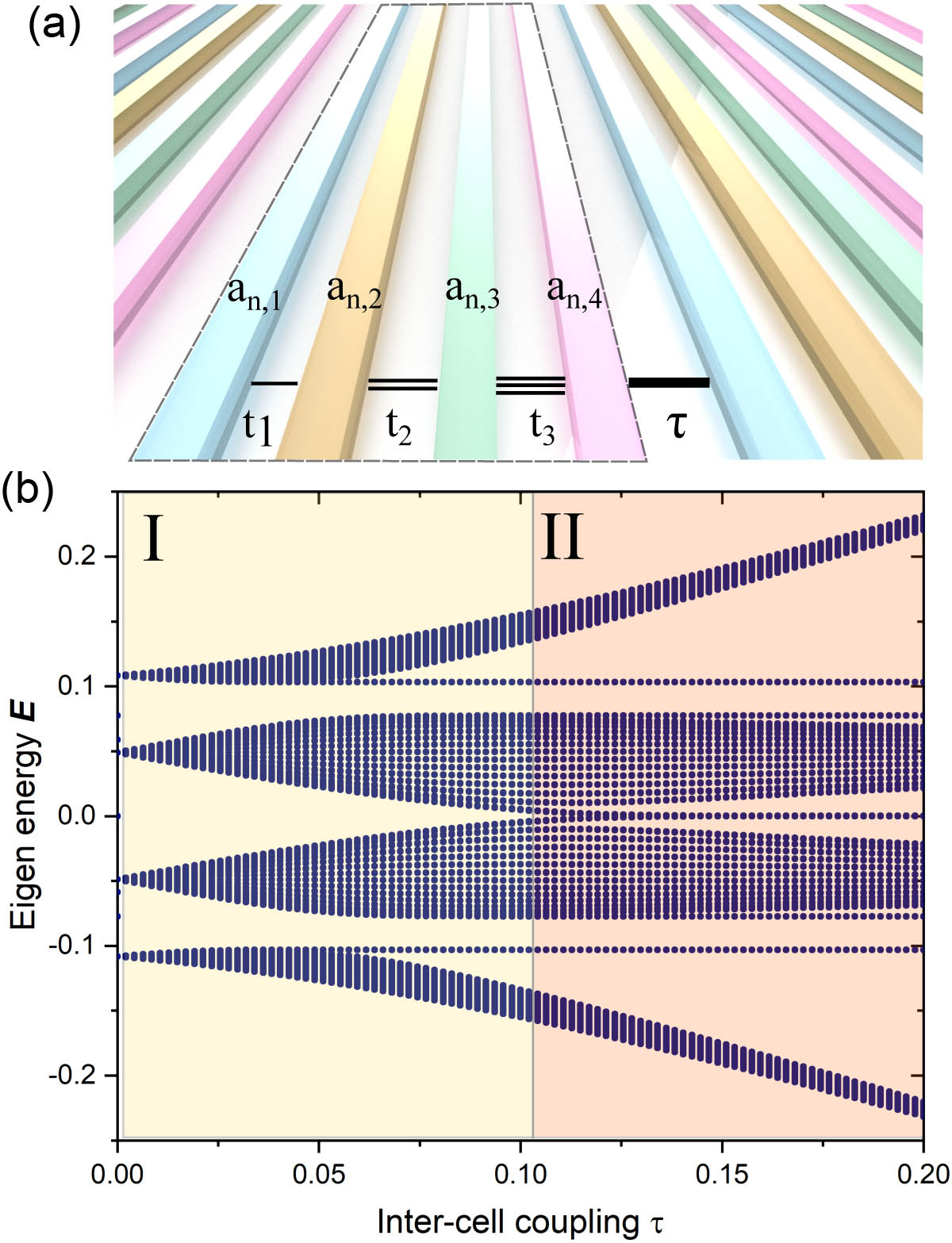
Figure 1.(a) Schematic of an superlattice. The lattice consists of four sites per unit cell, with intracell coupling amplitudes and intercell coupling amplitude . (b) Energy spectrum at different intercell coupling amplitude . The intracell coupling amplitudes are fixed at , , and . As the intercell coupling amplitude is increased, the first and third bandgaps never close. The situation is different for the bandgap centered at zero energy, where we can see the closure and reopening of the bandgap at together with the appearance of energy-degenerate right and left edge localized topologically protected states. Two regions are highlighted I and II, which correspond to the topologically trivial and nontrivial bandgap number , respectively.
The Hamiltonian in Eq. (1) can exhibit topologically nontrivial values in all three bandgaps for a superlattice with inversion symmetry satisfying . Alternatively, in the case of broken inversion symmetry only shows topologically protected quantized values for different intercell coupling , which is not the case for and . Figure 1(b) shows a simulated band structure of our superlattice with 15 cells; as the intercell coupling amplitude is tuned, the intracell coupling amplitudes are kept constant at , , and . We notice that the first and third bandgaps never close, with the emergence of left and right edge nontopological states within the bandgap at different energies. The case is different for the bandgap centered at zero energy, where we can see the closing and reopening of the bandgap at , with the emergence of energy-degenerate right and left edge localized topologically protected states in the superlattice. The bandgap number takes quantized values of and , for smaller and larger than , respectively. For an arbitrary input to the lattice, the beam displacement can be utilized to quantify the deviation of the light beam from the center point as light propagates in the lattice. can be directly related to the Zak phase of the band using a Wannier function. Such an input can uniformly excite the lowest -bands of the superlattice:
As this is rather challenging to achieve experimentally, it was shown in Ref. [22] that bulk excitation in a superposition state of the first and third waveguides in the central cell can predict the topological phase through the beam displacement measurement. The beam displacement then takes two quantized values:
For the superlattice parameters in Fig. 1(b), . Figures 2(a) and 2(b) show the simulated light evolution in two superlattices with different intercell coupling and , respectively. Each superlattice consists of 15 cells, among which the bulk eighth cell was used for excitation ; only the first and third waveguides in the central cell are excited equally and in phase. Figure 2(c) presents the numerically calculated beam displacement using Eq. (3) for different propagation lengths. The results confirm the theoretical prediction of quantized values of the beam displacement corresponding to the topological nature of the second bandgap number . The dotted lines in Fig. 2(d), corresponding to the left axis, show calculated beam displacement at propagation distance of 200 μm versus the phase difference between the two excited sites, for the two superlattices in Figs. 2(a) and 2(b). The solid line, corresponding to the right axis, shows the difference between the beam displacement in the trivial and nontrivial superlattices. The result indicates that, even for large variations in the input phase, there is a clear distinction between the beam displacement measurement for different topological phases, making the experimental realization both robust and feasible.
Figure 2.(a), (b) Simulated light evolution pattern in superlattices. The two superlattices have the same parameters as in Fig. 1(a) band diagram, with () in (a) and () in (b), corresponding to topologically trivial and nontrivial phases, respectively. Bulk excitation is used at the eighth cell . (c) Beam displacement calculation of trivial superlattice (gold) and nontrivial superlattice (brown). The numerical calculation involves summing over all the superlattice cells at different propagation distances using Eq. (3). Two quantized values of 0 and −0.25 are found in the case of trivial and nontrivial superlattices. (d) Phase difference versus beam displacement. The beam displacement (dotted lines, left axis) is calculated for different phases between the two input waveguides , for the trivial phase (gold) and the nontrivial lattice (brown). The difference between the two beam displacements in the trivial and nontrivial superlattices is shown by the green solid line (right side axis) with robustness.
3. EXPERIMENTAL MEASUREMENT OF TOPOLOGICAL INVARIANTS
A CMOS-compatible photonic platform [31,32] is used to implement the engineered superlattices. Each waveguide representing a superlattice site has a dimension of , with and poly(methyl methacrylate) (PMMA) as the bottom and top cladding, respectively. Mode simulations are used to calculate the superlattice site spacings to satisfy the nearest neighbor coupling amplitudes in the model [33]. Two superlattices were fabricated with identical intracell spacings , , and , while having two distinct intercell spacings and , corresponding to the topologically trivial and nontrivial phases. The experimental setup is shown in Fig. 3(a). We excite the superlattice using a continuous-wave laser source centered at 795 nm. A lensed fiber installed on a five-axis nanopositioning stage is used to couple the light to the nanophotonic chip. A polarizing beam splitter and a fiber-coupled three-paddle polarization controller are used to selectively excite the transverse electric (TE) mode of the waveguide. An on-chip Y-splitter divides the input light into two pathways. The first leads to the superlattice, while the second acts as a monitor for the coupling efficiency and the polarization on-chip. A charge-coupled device (CCD) camera with a 40× objective is used to image the evolution pattern of the light along the propagation.
Figure 3.Schematic of the experimental setup. A 795 nm CW laser is used to excite the chip via a lensed fiber, and the TE mode of the waveguide is selected with a polarization controller. To confirm the excited mode polarization in the superlattice, the chip’s output is free-space-coupled to an optical power meter after a polarizing beam splitter. A microscope equipped with a CCD camera is used to top-image the light dispersed from the superlattice. To measure the light dynamics in the photonic lattice, nanoscattering structures are introduced to the odd and even cells in the lattice [34], separated by a distance of 5 μm. The inset shows the top image of the lattice, where the top and bottom rows sample the light propagating in the odd and even cells, respectively. In total, the device has a length of 300 μm, with five sampling sections measured at distances of 40, 80, 120, 160, and 200 μm. (b) False colored SEM image of integrated photonic chip. The input waveguide branches to the superlattice (yellow) and the reference port (green). A 50:50 Y-shaped beam splitter (blue) is used to excite the superlattice in the state. (c) Magnified SEM image of the nanoscattering structures at the odd and even cells to sample the light intensity in the superlattice. The dotted white boxes indicate the location of the nanoscattering structure. The scale bars in (b) and (c) correspond to lengths of 40 μm and 2 μm, respectively.
It is technically challenging to detect light intensity in individual nanosized waveguides using an optical microscope since the superlattice dimensions and spacings are below the Abbe diffraction limitation. Here, we deliberately introduce nanoscattering sites, in particular 50 nm gaps in the waveguides to scatter light upward toward the imaging system, providing means to sample the light intensity at a specific propagation length in the superlattice. To preserve the state fidelity in the superlattice, the nanoscattering structures are introduced in all the odd and even cells, separated by 5 μm, which is a length scale well below the coupling lengths in the system. The inset of Fig. 3(a) shows a top image of the superlattice, where the top (bottom) row gives an intensity measurement of the light in the odd (even) cells. Using this approach, the beam displacement is calculated using Eq. (3) by summing over the odd and even cell numbers. Figure 3(b) shows a false colored scanning electron microscope (SEM) image of the superlattice (yellow), integrated with a 50:50 beam splitter (green) to excite a superposition state at the eighth cell. A reference waveguide (green) is used to measure the transmitted light off-chip using a 100× objective. Figure 3(c) shows a false colored SEM image of different cells, and the scattering nanostructures are highlighted in white.
Higher spatial frequency of the nanoscattering structures would enable higher resolution probing of the light propagation dynamics, with a compromise of faster exponential decay of light intensity in the superlattice. The total superlattice length is selected to be 300 μm, with five intensity samples taken at a period of 40 μm, which provides a balance between the resolution and efficiency. Top images of both the trivial and nontrivial superlattices are recorded, and the intensity distributions in the odd and even cells are extracted and normalized. Figures 4(a) and 4(b) show simulated (black dashed line) and measured light intensity in different cells for the trivial (gold dotted line) and nontrivial (brown dotted line) superlattices, respectively. Larger spread can be seen for the trivial case, with a good agreement between simulation and measurement. Note that no free fitting parameters are used in Figs. 4(a) and 4(b), and the coupling amplitudes in the Hamiltonian are directly determined from the physical parameters of the lattice. Figure 4(c) shows the extracted beam displacement using Eq. (3), integrated over the cells. Using the two-waveguide bulk excitation approach, we observe beam displacement of 0.088 in the case of trivial photonic superlattices, and in the case of nontrivial photonic superlattices. This is in excellent agreement with the theoretical values of 0 and . Possible deviations in the measured values can be attributed to the imbalanced splitting ratio and phase in the 50:50 beam splitter due to fabrication inaccuracy, specifically the electron beam lithography and reactive ion etching. The experimentally measured topologically invariant is comparable to the winding number introduced in Ref. [35] for the system, while we introduce an experimentally feasible approach that does not require measuring chiral average displacements.
Figure 4.(a), (b) Light intensity over different cells in topologically trivial and nontrivial superlattices, respectively. The experimental data are shown by the dotted lines, while the solid lines represent the numerically modeled superlattice. The coupling amplitudes in the simulated Hamiltonian are directly determined from the chip physical dimensions and refractive indices of different materials; no free fitting parameters are utilized. As the propagation distance increases, the trivial superlattice has greater spread around the input eighth cell. (c) Experimentally measured beam displacement. Measured topological invariant of the trivial superlattice (gold) and nontrivial superlattice (brow) at different propagation distances. The beam displacement is evaluated through integrating the intensity multiplied by the cell numbers over the cell numbers in Eq. (3). In the case of the trivial photonic superlattices, we measure a beam displacement of 0.088, while in the case of nontrivial photonic superlattices, . The results show good agreement with the theoretical values (dotted lines) of 0 and . A distinct gap can be observed for the different topological phases.
In summary, we directly probe the topology of chiral superlattices with broken inversion symmetry using a CMOS-compatible nanophotonic device, relying on a superposition state excitation. For the trivial and nontrivial phase photonic superlattices, our measurements reveal quantized beam displacements in close agreement with the theoretical models. A major goal in topological physics is relating global topological invariants with experimentally measurable quantities. Our method of introducing nanoscattering sites to study the light dynamics in the superlattice, offers a novel single-shot identification of quantized topological numbers, opening the path for direct measurements of topological invariants in more complex photonic structures and the implementation of topologically protected multi-band devices.
Acknowledgment
Acknowledgment. A. W. E acknowledges support from the Knut and Alice Wallenberg (KAW) Foundation through the Wallenberg Centre for Quantum Technology (WACQT), Swedish Research Council (VR) Starting, and Vinnova quantum kick-start project 2021. S. S. acknowledges support from VR Starting. V. Z. acknowledges support from the KAW and VR.
APPENDIX A: CHIP DESIGN PARAMETERS
Following the theoretical model in Section 2, we design a chip based on the silicon nitride () platform to realize our single-shot detection method. The thickness is 250 nm, and the width of the waveguides is 500 nm. Each site in the unit cell consists of a single waveguide, with bottom PMMA top cladding. We perform ellipsometry measurements to characterize the refractive index of and with excellent accuracy. The blue and green curves in Fig. 5 represent the measured refractive indices for wavelengths between 700 nm and 1000 nm. The light blue and green squares indicate the refractive indices at the operating wavelength of 795 nm. The data were used to determine the design parameters and engineer the coupling strengths in the photonic lattices.
Figure 5.Refractive indices measured by ellipsometry. The measurement is performed for wavelengths between 700 nm and 1000 nm, at 5 nm steps. The blue curve shows the refractive index of , while the green curve shows the refractive index of the cladding. The operating wavelength of the device is highlighted at 795 nm.
Figure 6.Coupling strength between the waveguides. (a) and (b) show the real component of the electric field for the odd and even TE modes supported in a waveguide dimer. (c) Coupling strength per micrometer between two waveguides for different gaps. The simulated data are fitted according to Eq. (A1) with a decay constant of μ.
Ze-Sheng Xu, Jun Gao, Govind Krishna, Stephan Steinhauer, Val Zwiller, Ali W. Elshaari, "Direct measurement of topological invariants in photonic superlattices," Photonics Res. 10, 2901 (2022)