
P. Boucaud, M. El Kurdi, A. Ghrib, M. Prost, M. de Kersauson, S. Sauvage, F. Aniel, X. Checoury, G. Beaudoin, L. Largeau, I. Sagnes, G. Ndong, M. Chaigneau, R. Ossikovski, "Recent advances in germanium emission [Invited]," Photonics Res. 1, 102 (2013)
- Photonics Research
- Vol. 1, Issue 3, 102 (2013)
![Calculated dependence of photoinduced carrier density needed to reach transparency at room temperature in n-doped germanium as a function of tensile strain. The germanium doping is 2×1019 cm−3. The calculation is based on the 30-band k·p formalism that we presented in [16]. The squares account for free-carrier absorption, as reported in [13]. The circles correspond to a calculation that considers the experimental absorption cross section for electrons and holes reported in [20] and a power law dependence as a function of wavelength with an exponent of 2.25 for electrons and 2.43 for holes.](/richHtml/prj/2013/1/3/03000102/img_001.jpg)
Fig. 1. Calculated dependence of photoinduced carrier density needed to reach transparency at room temperature in n 2 × 10 19 cm − 3 k · p
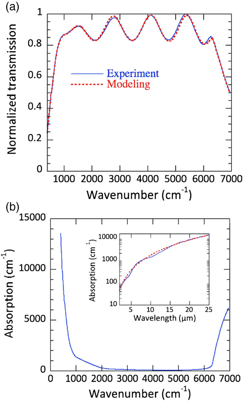
Fig. 2. (a) Transmission of a Ge/GaAs film normalized by the transmission of a GaAs wafer. Both wafers are double-side polished. The germanium thickness is 930 nm. The doping of the germanium layer is 10 19 cm − 3 absorption ∝ λ 2.25
Fig. 3. (a) Scanning electron microscopy image of tensile-strained germanium microdisk. (b) Room temperature photoluminescence spectrum of an unstrained (bottom) and strained (top) germanium microdisk with a 4 μm diameter. (c) Enlargement of the emission around 2000 nm [48].
Fig. 4. (a) In-plane strain map of the germanium microdisk as deduced from backscattering μ 1 , only one component is considered to describe the strain.
Fig. 5. (a) Conduction band profile of a GaAs/Ge/GaAs heterostructure without applied bias. (b) Conduction band profile for a 1.5 V applied bias. The quasi-Fermi levels are indicated by dashed lines.


Set citation alerts for the article
Please enter your email address

© Copyright 2018-2021 | Chinese Laser Press. All Rights Reserved 沪ICP备15018463号-20