• Photonics Research
  • Vol. 8, Issue 10, A50 (2020)
Michal Baranowski1, Paulina Plochocka1、2, Rui Su3, Laurent Legrand4, Thierry Barisien4, Frederick Bernardot4, Qihua Xiong3, Christophe Testelin4, and Maria Chamarro4、*
Author Affiliations
  • 1Department of Experimental Physics, Faculty of Fundamental Problems of Technology, Wroclaw University of Science and Technology, Wroclaw, Poland
  • 2Laboratoire National des Champs Magnétiques Intenses, UPR 3228, CNRS-UGA-UPS-INSA, Grenoble and Toulouse, France
  • 3Division of Physics and Applied Physics, School of Physical and Mathematical Sciences, Nanyang Technological University, Singapore, Singapore
  • 4Sorbonne Université, CNRS-UMR 7588, Institut des NanoSciences de Paris, INSP, Paris, France
  • show less
    DOI: 10.1364/PRJ.401872 Cite this Article Set citation alerts
    Michal Baranowski, Paulina Plochocka, Rui Su, Laurent Legrand, Thierry Barisien, Frederick Bernardot, Qihua Xiong, Christophe Testelin, Maria Chamarro. Exciton binding energy and effective mass of CsPbCl3: a magneto-optical study[J]. Photonics Research, 2020, 8(10): A50 Copy Citation Text show less
    (a) Typical optical microscopy (reflection configuration) image of a CsPbCl3∼250 nm thick film grown on muscovite mica following the method reported in Refs. [32,33]. (b) Optical transmittance of the film shown in (a) at 2 K and zero magnetic field. S1 and S2 correspond, respectively, to the n=1 and 2 exciton states in the hydrogenic model. (c) Optical transmittance of the film shown in (a) at RT.
    Fig. 1. (a) Typical optical microscopy (reflection configuration) image of a CsPbCl3250  nm thick film grown on muscovite mica following the method reported in Refs. [32,33]. (b) Optical transmittance of the film shown in (a) at 2 K and zero magnetic field. S1 and S2 correspond, respectively, to the n=1 and 2 exciton states in the hydrogenic model. (c) Optical transmittance of the film shown in (a) at RT.
    (a) Optical transmittance of the CsPbCl3 film shown in Fig. 1(a) at 2 K for different magnetic field values. The pulsed magnetic field is perpendicular to the film (Faraday configuration). (b) The energy position of S1 (n=1) and S2 (n=2) versus magnetic field. Parabolic fits to the data according to Eq. (2) in the main text lead to geff=0.8 and diamagnetic shift coefficients σXn of 0.64 μeV/T2 and 2.0 μeV/T2 for n=1 and 2, respectively.
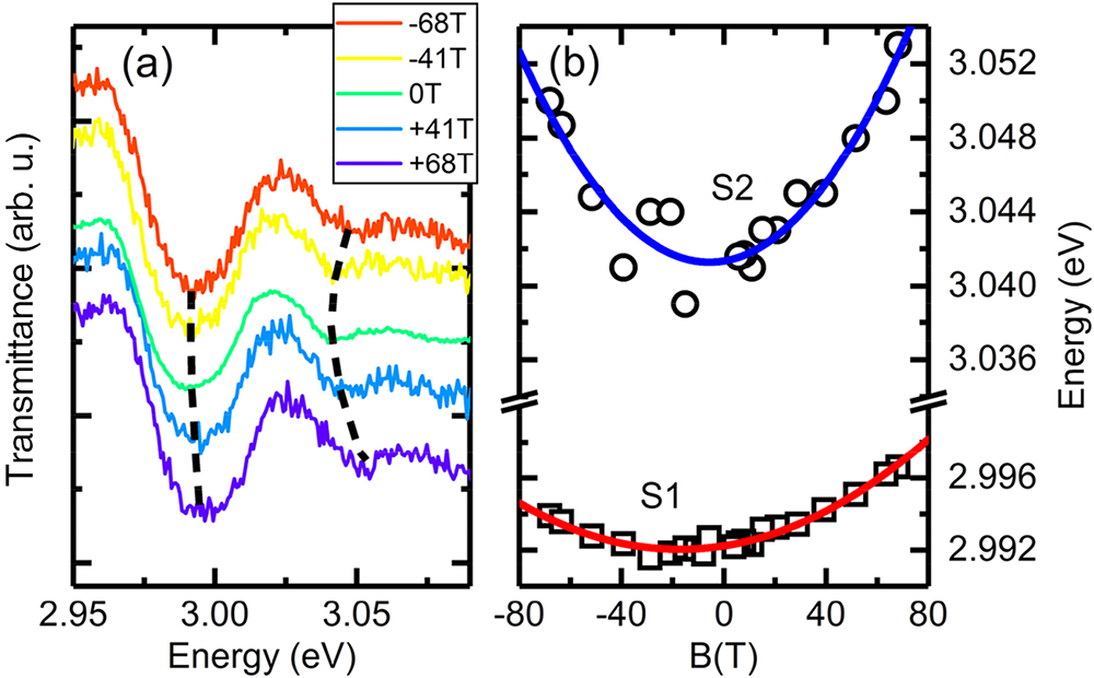
    Fig. 2. (a) Optical transmittance of the CsPbCl3 film shown in Fig. 1(a) at 2 K for different magnetic field values. The pulsed magnetic field is perpendicular to the film (Faraday configuration). (b) The energy position of S1 (n=1) and S2 (n=2) versus magnetic field. Parabolic fits to the data according to Eq. (2) in the main text lead to geff=0.8 and diamagnetic shift coefficients σXn of 0.64  μeV/T2 and 2.0  μeV/T2 for n=1 and 2, respectively.
    (a) Exciton reduced mass, (b) exciton binding energy, and (c) effective dielectric constant as functions of the energy gap. Measurements are done at 2 K. Full orange stars correspond to CsPbX3 with X=I, Br or to CsPbI2Br [37]. Empty orange stars correspond to CsPbCl3 (this work). Open green squares represent results for the MA and formamindinium (FA) iodides, bromides, or mixed halide (green square at 1.596 eV is for I3−xClx) [38]. Open red squares correspond to MAPb1−xSnxI3 [41]. Black solid line in (a) is a linear fit to the data. Vertical dashed green line indicates the value of the energy gap at which a maximum of the effective dielectric constant is found for the considered perovskite compounds.
    Fig. 3. (a) Exciton reduced mass, (b) exciton binding energy, and (c) effective dielectric constant as functions of the energy gap. Measurements are done at 2 K. Full orange stars correspond to CsPbX3 with X=I, Br or to CsPbI2Br [37]. Empty orange stars correspond to CsPbCl3 (this work). Open green squares represent results for the MA and formamindinium (FA) iodides, bromides, or mixed halide (green square at 1.596 eV is for I3xClx) [38]. Open red squares correspond to MAPb1xSnxI3 [41]. Black solid line in (a) is a linear fit to the data. Vertical dashed green line indicates the value of the energy gap at which a maximum of the effective dielectric constant is found for the considered perovskite compounds.
    (a) Exciton binding energy EX and (b) Bohr radius aX versus the gap energy of halide-based perovskites and other semiconductors with different crystalline structures, either zinc blende, wurtzite, or diamond. The solid lines correspond to fits with, respectively, EX∝Eg1.62 and aX∝Eg−1.33. Perovskite values are given in Table 1. InAs and ZnO [46], GaAs [47], ZnTe [48], ZnS [49], AlN [50], and the other semiconductors [51].
    Fig. 4. (a) Exciton binding energy EX and (b) Bohr radius aX versus the gap energy of halide-based perovskites and other semiconductors with different crystalline structures, either zinc blende, wurtzite, or diamond. The solid lines correspond to fits with, respectively, EXEg1.62 and aXEg1.33. Perovskite values are given in Table 1. InAs and ZnO [46], GaAs [47], ZnTe [48], ZnS [49], AlN [50], and the other semiconductors [51].
    CompoundEg (eV)EX (meV)m0εrgeff
    bCsPbCl33.05664±1.50.202±0.016.56±0.240.8
    cCsPbBr32.34233±10.126±0.017.3
    cCsPbI31.72315±10.114±0.0110.0
    dFAPbBr32.233220.1158.42
    dFAPbI31.501140.099.352.3
    dMAPbBr32.292250.1177.5
    dMAPbI31.652160.1049.4e1.2
    Table 1. Exciton Parameters in the Family of Halide Perovskite Compounds Deduced from Magneto-Optical Experiments at 2 Ka
    Michal Baranowski, Paulina Plochocka, Rui Su, Laurent Legrand, Thierry Barisien, Frederick Bernardot, Qihua Xiong, Christophe Testelin, Maria Chamarro. Exciton binding energy and effective mass of CsPbCl3: a magneto-optical study[J]. Photonics Research, 2020, 8(10): A50
    Download Citation