• Chinese Physics B
  • Vol. 29, Issue 9, (2020)
Bo-Bo Tian1、†, Ni Zhong1, and Chun-Gang Duan1、2
Author Affiliations
  • 1Key Laboratory of Polar Materials and Devices (MOE), Department of Electronics, East China Normal University, Shanghai 20024, China
  • 2Collaborative Innovation Center of Extreme Optics, Shanxi University, Shanxi 030006, China
  • show less
    DOI: 10.1088/1674-1056/aba603 Cite this Article
    Bo-Bo Tian, Ni Zhong, Chun-Gang Duan. Recent advances, perspectives, and challenges in ferroelectric synapses[J]. Chinese Physics B, 2020, 29(9): Copy Citation Text show less
    (a) Typical multiple polarization (P) versus voltage loops under various voltage amplitudes obtained from an Au/PVDF/Al capacitor. (b) Schematic illustration of multiple domains states in a ferroelectric film. (c) Sketch of a synapse.
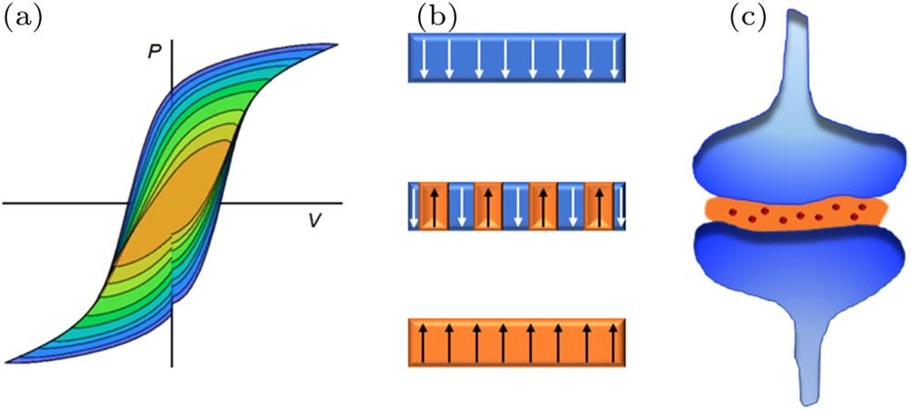
    Fig. 1. (a) Typical multiple polarization (P) versus voltage loops under various voltage amplitudes obtained from an Au/PVDF/Al capacitor. (b) Schematic illustration of multiple domains states in a ferroelectric film. (c) Sketch of a synapse.
    Schematic representation of the energy potential profile in an FTJ for polarization pointing to the electrode one (Metal1) (a) and for polarization pointing to the electrode two (Metal2) (b). Reproduced from Ref. [7], copyright 2005, with permission of APS.
    Fig. 2. Schematic representation of the energy potential profile in an FTJ for polarization pointing to the electrode one (Metal1) (a) and for polarization pointing to the electrode two (Metal2) (b). Reproduced from Ref. [7], copyright 2005, with permission of APS.
    (a) Evolution of the junction resistance and ferroelectric domain configuration in a 180 nm wide (Ca,Ce)MnO3/BiFeO3/Pt/Co FTJ. (b) Symbols are experimental resistance as a function of percentage of down domains extracted from the PFM phase images and the black curve is a simulation in a parallel resistance model shown in inset. Reproduced from Ref. [24], copyright 2013, with permission of ACS.
    Fig. 3. (a) Evolution of the junction resistance and ferroelectric domain configuration in a 180 nm wide (Ca,Ce)MnO3/BiFeO3/Pt/Co FTJ. (b) Symbols are experimental resistance as a function of percentage of down domains extracted from the PFM phase images and the black curve is a simulation in a parallel resistance model shown in inset. Reproduced from Ref. [24], copyright 2013, with permission of ACS.
    The FTJ could be treated as a two-terminal synapse where the top and bottom electrodes transmit signals from pre and post neurons. (a) Sketch of pre- and post-neurons connected by a synapse. (b) Sketch of the (Ca,Ce)MnO3/BiFeO3/Pt/Co FTJ. YAO stands for YAlO3. (c) Single-pulse hysteresis loop of the resistance versus voltage amplitude, there are voltage thresholds ± Vth beyond which resistive switching occurs. (d) Measurements of STDP in the FTJ. The junction conductance increases or decreases depending on the timing and causality of pre and post electrical signals. The insets show the waveforms produced by the superposition of presynaptic and postsynaptic spikes. Reproduced from Ref. [43], copyright 2014, with permission of Springer Nature.
    Fig. 4. The FTJ could be treated as a two-terminal synapse where the top and bottom electrodes transmit signals from pre and post neurons. (a) Sketch of pre- and post-neurons connected by a synapse. (b) Sketch of the (Ca,Ce)MnO3/BiFeO3/Pt/Co FTJ. YAO stands for YAlO3. (c) Single-pulse hysteresis loop of the resistance versus voltage amplitude, there are voltage thresholds ± Vth beyond which resistive switching occurs. (d) Measurements of STDP in the FTJ. The junction conductance increases or decreases depending on the timing and causality of pre and post electrical signals. The insets show the waveforms produced by the superposition of presynaptic and postsynaptic spikes. Reproduced from Ref. [43], copyright 2014, with permission of Springer Nature.
    (a) STDP measurement in La0.7Sr0.3MnO3/BaTiO3/La0.7Sr0.3MnO3 MTJ with the parallel (p) or antiparallel (AP) states of magnetization alignment in electrodes. (b) Schematic illustration of the magnetoelectrically coupled memristor and the corresponding synapses. Reproduced from Ref. [44], copyright 2018, with permission of ACS.
    Fig. 5. (a) STDP measurement in La0.7Sr0.3MnO3/BaTiO3/La0.7Sr0.3MnO3 MTJ with the parallel (p) or antiparallel (AP) states of magnetization alignment in electrodes. (b) Schematic illustration of the magnetoelectrically coupled memristor and the corresponding synapses. Reproduced from Ref. [44], copyright 2018, with permission of ACS.
    (a) Ferroelectricity in ultrathin thin films of PVDF. Topography (top), PFM phase (middle), and amplitude (bottom) images, after switching the polarisation upward in the central 5 × 5 μm2 area of a 2 L-thick (left) and 1 L-thick (right) PVDF films. Scale bar, 1 mm. (b) Three-dimensional schematic diagram of PVDF FTJs. (c) I–V curves in the 1 L and 2 L PVDF FTJs. The arrows show the direction of the voltage sweeps. (d) Local PFM phase and (e) voltage dependences of the TER of an Au/PVDF (1 L)/W junction (left) and an Au/PVDF (2 L)/W junction (right), respectively. The vertical dashed lines show the agreement between polarization and resistance coercive voltages. Reproduced from Ref. [37], copyright 2016, with permission of Springer Nature.
    Fig. 6. (a) Ferroelectricity in ultrathin thin films of PVDF. Topography (top), PFM phase (middle), and amplitude (bottom) images, after switching the polarisation upward in the central 5 × 5 μm2 area of a 2 L-thick (left) and 1 L-thick (right) PVDF films. Scale bar, 1 mm. (b) Three-dimensional schematic diagram of PVDF FTJs. (c) IV curves in the 1 L and 2 L PVDF FTJs. The arrows show the direction of the voltage sweeps. (d) Local PFM phase and (e) voltage dependences of the TER of an Au/PVDF (1 L)/W junction (left) and an Au/PVDF (2 L)/W junction (right), respectively. The vertical dashed lines show the agreement between polarization and resistance coercive voltages. Reproduced from Ref. [37], copyright 2016, with permission of Springer Nature.
    (a) Evolution of the junction resistance as a function of voltage amplitude in an Au/P(VDF-TrFE)/Nb:SrTiO3 FTJ. (c), (d) Programmable conductance, corresponding to LTP/D of synaptic weight, is achieved by modulating either amplitude (b) or number (c) of applied voltage pulses. (d) Measurements of LTP/D. (e) Measurements of Hebbian and anti-Hebbian STDP learning rules. Reproduced from Ref. [40], copyright 2019, with permission of John Wiley and Sons.
    Fig. 7. (a) Evolution of the junction resistance as a function of voltage amplitude in an Au/P(VDF-TrFE)/Nb:SrTiO3 FTJ. (c), (d) Programmable conductance, corresponding to LTP/D of synaptic weight, is achieved by modulating either amplitude (b) or number (c) of applied voltage pulses. (d) Measurements of LTP/D. (e) Measurements of Hebbian and anti-Hebbian STDP learning rules. Reproduced from Ref. [40], copyright 2019, with permission of John Wiley and Sons.
    (a) Sketch of Pt/BaTiO3/Nb:SrTiO3 FTJs. (b) Linear and symmetric conductance update with 200 states and 500 reproducible cycles. (c) Schematic diagram of a three layers neural network (left) and neural core with a crossbar structure to perform the analog matrix operations (right). (d) The simulation results, the training accuracy of BaTiO3 FTJs and SrTiO3 based resistive devices for a small image (left) and a large image (right). Reproduced from Ref. [45], copyright 2019, with permission of John Wiley and Sons.
    Fig. 8. (a) Sketch of Pt/BaTiO3/Nb:SrTiO3 FTJs. (b) Linear and symmetric conductance update with 200 states and 500 reproducible cycles. (c) Schematic diagram of a three layers neural network (left) and neural core with a crossbar structure to perform the analog matrix operations (right). (d) The simulation results, the training accuracy of BaTiO3 FTJs and SrTiO3 based resistive devices for a small image (left) and a large image (right). Reproduced from Ref. [45], copyright 2019, with permission of John Wiley and Sons.
    (a) The schematic diagram of high-density 3D vertical HZO-based FTJS array with high resolution transmission electron microscopy image of the 3D TiN/ HZO/Pt devices. (b) Measurements of Hebbian and anti-Hebbian STDP rule in the HZO-based synaptic array. The red lines are the exponential fits to the experimental data. (c) The schematic diagram of multilayer perceptron network (left), and simulated output signal in which “correct” class of the applied letter patterns is larger than the other “false” outputs after learning process (right). Reproduced from Ref. [36], copyright 2018, with permission of RSC.
    Fig. 9. (a) The schematic diagram of high-density 3D vertical HZO-based FTJS array with high resolution transmission electron microscopy image of the 3D TiN/ HZO/Pt devices. (b) Measurements of Hebbian and anti-Hebbian STDP rule in the HZO-based synaptic array. The red lines are the exponential fits to the experimental data. (c) The schematic diagram of multilayer perceptron network (left), and simulated output signal in which “correct” class of the applied letter patterns is larger than the other “false” outputs after learning process (right). Reproduced from Ref. [36], copyright 2018, with permission of RSC.
    (a) Schematic diagram of charge distribution and energy-band diagrams of a Pt/BiFeO3/Nb:SrTiO3 FD at low resistance state. (b) Schematic diagram of charge distribution and energy-band diagrams of a Pt/BiFeO3/ Nb:SrTiO3 FD at high resistance state. Reproduced from Ref. [68], copyright 2013, with permission of AIP Publishing.
    Fig. 10. (a) Schematic diagram of charge distribution and energy-band diagrams of a Pt/BiFeO3/Nb:SrTiO3 FD at low resistance state. (b) Schematic diagram of charge distribution and energy-band diagrams of a Pt/BiFeO3/ Nb:SrTiO3 FD at high resistance state. Reproduced from Ref. [68], copyright 2013, with permission of AIP Publishing.
    (a) Schematic diagram of Au/BaTiO3/SmNiO3 FDs. (b) Off-pulse R–Vwrite curves in an Au/BaTiO3/SmNiO3 FD. (c) DC I–V curves in an Au/BaTiO3/SmNiO3 FD. (d) Local PFM hysteresis loops of an Au/BaTiO3/SmNiO3 FD. Reproduced from Ref. [76], copyright 2019, with permission of AIP Publishing.
    Fig. 11. (a) Schematic diagram of Au/BaTiO3/SmNiO3 FDs. (b) Off-pulse RVwrite curves in an Au/BaTiO3/SmNiO3 FD. (c) DC IV curves in an Au/BaTiO3/SmNiO3 FD. (d) Local PFM hysteresis loops of an Au/BaTiO3/SmNiO3 FD. Reproduced from Ref. [76], copyright 2019, with permission of AIP Publishing.
    (a) The lower half part is out-of-plane phase image and the upper half part is the corresponding current mapping with read voltage of –0.5 V measured on BiFeO3/SrRuO3/ SrTiO3 (substrate). (b) Out-of-plane phase images after heating the sample at 25 °C, 300 °C, and 500 °C for 5 min, respectively. (c) R–V hysteresis loops of an Au/BiFeO3/SrRuO3 FD at –170 °C, 25 °C, 100 °C, 200 °C, and 300 °C, respectively. Reproduced from Ref. [69], copyright 2019, with permission of IOP Publishing.
    Fig. 12. (a) The lower half part is out-of-plane phase image and the upper half part is the corresponding current mapping with read voltage of –0.5 V measured on BiFeO3/SrRuO3/ SrTiO3 (substrate). (b) Out-of-plane phase images after heating the sample at 25 °C, 300 °C, and 500 °C for 5 min, respectively. (c) RV hysteresis loops of an Au/BiFeO3/SrRuO3 FD at –170 °C, 25 °C, 100 °C, 200 °C, and 300 °C, respectively. Reproduced from Ref. [69], copyright 2019, with permission of IOP Publishing.
    (a) Schematic structure of an HZO FeFET. (b) Transfer curve of the HZO FeFET. (c) LTP/D properties of the HZO FeFET with incremental pulse scheme. (d) Schematic illustration of two-layer perceptron neural network for simulation of pattern recognition. Reproduced from Ref. [83], copyright 2019, with permission of ACS.
    Fig. 13. (a) Schematic structure of an HZO FeFET. (b) Transfer curve of the HZO FeFET. (c) LTP/D properties of the HZO FeFET with incremental pulse scheme. (d) Schematic illustration of two-layer perceptron neural network for simulation of pattern recognition. Reproduced from Ref. [83], copyright 2019, with permission of ACS.
    (a) Sketch of a biological synapse. (b) Sketch of an MoS2 FeFET with ferroelectric P(VDF-TrFE) gate insulator. Note that the input port can be either the gate-source/drain port or the drain-source port. For supervised learning in general SNN, the channel usually connects pre and post synaptic neurons while the gate terminal accepts signals to modulate the channel conductance. (c) Channel conductance versus gate electric field curves in a MoS2 FeFET. (d) Gate current versus gate electric field curve of the MoS2 FeFET. (e) Evolution of channel conductance as a function of the different voltage pulse sequences. (f) Measurements of Hebbian STDP learning rule in a MoS2 FeFET. Reproduced from Ref. [1], copyright 2019, with permission of John Wiley and Sons.
    Fig. 14. (a) Sketch of a biological synapse. (b) Sketch of an MoS2 FeFET with ferroelectric P(VDF-TrFE) gate insulator. Note that the input port can be either the gate-source/drain port or the drain-source port. For supervised learning in general SNN, the channel usually connects pre and post synaptic neurons while the gate terminal accepts signals to modulate the channel conductance. (c) Channel conductance versus gate electric field curves in a MoS2 FeFET. (d) Gate current versus gate electric field curve of the MoS2 FeFET. (e) Evolution of channel conductance as a function of the different voltage pulse sequences. (f) Measurements of Hebbian STDP learning rule in a MoS2 FeFET. Reproduced from Ref. [1], copyright 2019, with permission of John Wiley and Sons.
    (a) Schematic view that when the polarization is upward/downward, the graphene channel becomes hole/electron dominated due to different positions of Fermi levels within the graphene energy bands. (b) The channel conductance will be decreased/increased due to reduction/enhancement of hole/electron density caused by the corresponding change of ferroelectric polarization. (c) A remote supervise method (ReSuMe) module composed of graphene FeFET complementary synapses, leaky integrate-and-fire (LIF) neuron, and supervise circuits (left). Time chart of signals (right). (d) Sketch of single-layer perceptron for classification of 3 × 3 binary images of z, v, and n, where classification is represented by the different timings of the output neuron. (e) The simulation results, the evolution of output signals, where output timings for z, v, and n inputs gradually approach the desired timings labeled by dash lines. Reproduced from Ref. [85], copyright 2019, with permission of Springer Nature.
    Fig. 15. (a) Schematic view that when the polarization is upward/downward, the graphene channel becomes hole/electron dominated due to different positions of Fermi levels within the graphene energy bands. (b) The channel conductance will be decreased/increased due to reduction/enhancement of hole/electron density caused by the corresponding change of ferroelectric polarization. (c) A remote supervise method (ReSuMe) module composed of graphene FeFET complementary synapses, leaky integrate-and-fire (LIF) neuron, and supervise circuits (left). Time chart of signals (right). (d) Sketch of single-layer perceptron for classification of 3 × 3 binary images of z, v, and n, where classification is represented by the different timings of the output neuron. (e) The simulation results, the evolution of output signals, where output timings for z, v, and n inputs gradually approach the desired timings labeled by dash lines. Reproduced from Ref. [85], copyright 2019, with permission of Springer Nature.
    Ferroelectric gate insulatorChannelRatioStatesRetentionEnergySynaptic functionsYearRef.
    SrBi2Ta2O9Si281999[78]
    Pb(Zr,Ti)O3ZnO>105>10>105 sLTP/D, STDP, On-chip pattern recognition2014[79]
    HZOSi4532LTP/D, Simulation of image recognition2017[80]
    Si:HfO2Si332LTP/D, STDP2017[81]
    HZOSi4.98>32LTP/D, Simulation of pattern recognition2018[82]
    HZOIGZO14.465LTP/D, Simulation of pattern recognition2019[83]
    P(VDF-TrFE)Organic polymer104>104 s75 PJSTP*, LTP, EPSC#, Visual-perception2018[84]
    P(VDF-TrFE)MoS21041000>103 s< 1 fJLTP/D, STDP2019[1]
    P(VDF-TrFE)Graphene3.25050 nJComplementary synapses, Simulation of pattern classification2019[85]
    P(VDF-TrFE)Organic polymer582019[86]
    P(VDF-TrFE)Carbon-nanotube104100400 sEPSC, IPSC&, LTP/D, Simulation of image recognition2020[87]
    Table 1. Experimental results of FeFET synapses.
    RatioStatesRetentionEnergyEnduranceConcurrent learningHigh densityReported array
    FTJsgoodgoodgoodpoorpoornogoodyes
    FDsgoodgoodgoodpoorpoornogoodno
    FeFETsgoodgoodpoorgoodgoodyespooryes
    Table 2. Radar chart to summarize perspectives for the FTJs, FDs, and FeFETs as electronic synapses.
    Bo-Bo Tian, Ni Zhong, Chun-Gang Duan. Recent advances, perspectives, and challenges in ferroelectric synapses[J]. Chinese Physics B, 2020, 29(9):
    Download Citation