Zhexin Zhao1, Dylan S. Black1, R. Joel England2, Tyler W. Hughes1..., Yu Miao1, Olav Solgaard1, Robert L. Byer1 and Shanhui Fan1,*|Show fewer author(s)
Zhexin Zhao, Dylan S. Black, R. Joel England, Tyler W. Hughes, Yu Miao, Olav Solgaard, Robert L. Byer, Shanhui Fan, "Design of a multichannel photonic crystal dielectric laser accelerator," Photonics Res. 8, 1586 (2020)
Copy Citation Text
To be useful for most scientific and medical applications, compact particle accelerators will require much higher average current than enabled by current architectures. For this purpose, we propose a photonic crystal architecture for a dielectric laser accelerator, referred to as a multi-input multi-output silicon accelerator (MIMOSA), that enables simultaneous acceleration of multiple electron beams, increasing the total electron throughput by at least 1 order of magnitude. To achieve this, we show that the photonic crystal must support a mode at the point in reciprocal space, with a normalized frequency equal to the normalized speed of the phase-matched electron. We show that the figure of merit of the MIMOSA can be inferred from the eigenmodes of the corresponding infinitely periodic structure, which provides a powerful approach to design such devices. Additionally, we extend the MIMOSA architecture to electron deflectors and other electron manipulation functionalities. These additional functionalities, combined with the increased electron throughput of these devices, permit all-optical on-chip manipulation of electron beams in a fully integrated architecture compatible with current fabrication technologies, which opens the way to unconventional electron beam shaping, imaging, and radiation generation.
1. INTRODUCTION
Miniaturization of accelerators is a rapidly growing field [1–4]. Among them, dielectric laser accelerators (DLAs) accelerate charged particles using the evanescent fields of dielectric structures driven by femtosecond laser pulses [4–8]. Due to the high damage threshold of dielectric materials in the near-infrared, the acceleration gradient of DLAs can be more than 10 times higher than conventional radio-frequency accelerators [9–12]. Recent progress in the integration of DLAs with photonic circuits has enabled the development of chip-scale accelerators, [13–18], which promise to further increase the compactness and practicality of this scheme. For subrelativistic and moderately relativistic electrons, focusing provided by laser-driven techniques, such as alternating phase focusing [19,20], enables stable electron beam transport and acceleration for long distances.
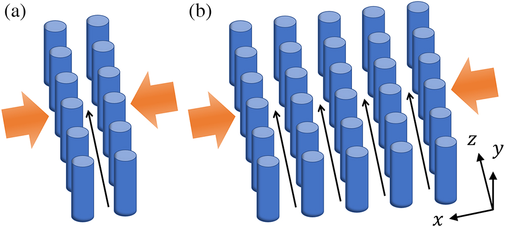
To promote the application of DLAs in both fundamental science and medical therapy [4,21,22], it is important to deliver high electron currents. However, since the geometric dimensions of currently existing DLA designs are on the wavelength scale, where the wavelength corresponds to that of their near-infrared drive lasers, it is intrinsically challenging to deliver an electron beam with high current through a single narrow electron channel as currently used in DLAs [19]. Motivated by this challenge, we explore a photonic crystal DLA architecture that has multiple electron channels (Fig. 1). We show that straightforward design principles lead to the electromagnetic fields inside different channels being almost identical, which enables simultaneous acceleration or manipulation of N phase-locked electron beams, increasing the total current by a factor of N.
Figure 1.Schematic of (a) a dual-pillar DLA and (b) a multichannel DLA. Two laser pulses (propagating in directions) incident on the DLA are indicated by the orange arrows. Electrons travel inside parallel channels along the direction.
Typical DLAs consist of a pair of dielectric gratings such as the dual silicon pillar DLAs illustrated in Fig. 1(a) [12]. When the laser beams illuminate the gratings, the near fields can be used to accelerate the electron beam that travels in the gap between two gratings. Although the height of the electron channel can be several micrometers, its width is limited to the submicrometer scale, due to the evanescent nature of the near fields. The small channel width limits the total electron current. To bypass this constraint, we propose a DLA architecture that consists of multiple parallel electron channels as shown in Fig. 1(b). The idea of simultaneous acceleration of multiple parallel beams has also been studied in millimeter wave accelerators [23–25]. However, the underlying physics and design principles of multichannel DLAs are fundamentally different from those of the millimeter-wave accelerators. Since each row of dielectric grating in the multichannel DLA is identical, this DLA structure is a finite photonic crystal. In contrast to previous single channel copropagating photonic crystal waveguide accelerators [26,27], our approach incorporates a multichannel design and operates based on side illumination to increase the total current. Consistent with Ref. [28], we focus on silicon pillars and refer this design as a multi-input multi-output silicon accelerator (MIMOSA).
Sign up for Photonics Research TOC. Get the latest issue of Photonics Research delivered right to you!Sign up now
We find that the essential characteristics of the MIMOSA are captured in the band structure and eigenmode properties of the underlying infinite photonic crystal. For simplicity, we study a two-dimensional photonic crystal with a rectangular lattice (Fig. 2), where the dielectric pillars extend uniformly in the direction. Previous studies confirm the validity of using a two-dimensional calculation to describe a photonic crystal with pillar height larger than the wavelength [28,29]. In a two-dimensional photonic crystal, the fields can be decomposed into TE (with , , and nonzero) and TM (with , , and nonzero) polarization [30]. Since only the TM polarization provides acceleration, we study only the TM polarization in this work. The unit cell and the band diagram of the photonic crystal underlying the MIMOSA are illustrated in Figs. 2(a) and 2(c), respectively. We assume that the electrons travel along the direction and are centered around and that the incident light propagates along the direction. Therefore, the incident laser can excite eigenmodes lying on the direction in the reciprocal space [Fig. 2(b)]. Furthermore, the mode at the point has the same phase in each unit cell. Thus, to ensure that the electron beams in different channels get the same acceleration, the mode at the point should be excited dominantly. Therefore, the frequency of the eigenmode at the point should match the frequency of the incident light. In addition, in order to satisfy the phase synchronization condition for the DLA [29,31], we need to have where is the speed of light, where is the speed of electron, is the periodicity along the direction, and is the diffraction order. In typical DLAs, the amplitude of the first-order diffraction is stronger than that of higher-order diffraction, so we take in the synchronization condition.
Figure 2.(a) Illustration of the photonic crystal where the unit cell is highlighted in the dashed red box. The electron propagation direction is indicated by the gray arrow. , , , and represent pillar length, pillar width, gap width, and the periodicity in the electron propagation direction, respectively. (b) The reciprocal Brillouin zone. (c) Band diagram of the TM mode of the photonic crystal with μ, μ, μ, and μ. Big (small) black dots represent eigenmodes with odd (even) mirror- symmetry, and red (blue) dots represent eigenmodes with even (odd) mirror- symmetry. (d), (e) Field profiles of the eigenmodes at the point with normalized frequency 0.500 and 0.411, respectively.
Additionally, the unit cell of typical photonic crystals may have certain symmetries. In the demonstration shown in Fig. 2, the mirror- and mirror- symmetries of the unit cell require that the acceleration mode should also have certain symmetries. To accelerate the electron traveling along , the mode should be symmetric with respect to the mirror plane [red dots in Fig. 2(c)]. And to couple to plane waves propagating in the direction, the mode should have odd mirror- symmetry. In other words, the photonic crystal underlying the MIMOSA should support an eigenmode at normalized frequency (frequency normalized by ) with odd mirror- and even mirror- symmetry; below we refer to such a mode as an acceleration mode. This condition on the symmetry of the acceleration mode, together with Eq. (1), represents one of the main contributions of this study and is referred to as the band structure condition below. It can be satisfied through tuning the geometrical parameters of the dielectric pillar.
Moreover, the figure of merit of the MIMOSA can also be derived from eigenmode analysis of the underlying photonic crystal. This “acceleration factor" [32–34] is the maximal acceleration gradient at the center of the electron channel divided by the maximal electric field inside the dielectric material. From the field profile of the acceleration mode [Fig. 2(d)], which is computed for a structure that is infinitely periodic along both the and directions, we can calculate the acceleration factor, which turns out to be close to the acceleration factor of the MIMOSA, where the structure is finite along the direction.
Based on the discussions above, the MIMOSA design procedure is summarized as follows. (1) Given the electron speed and the frequency of the excitation laser, the periodicity () of the photonic crystal along the electron propagation direction is determined by Eq. (1). (2) The periodicity along the transverse direction and the shape of the dielectric pillar in the unit cell can be tuned such that the band structure condition is satisfied and the width of the electron channel exceeds a value set by experimental considerations. (3) Using the acceleration factor of the acceleration mode as the objective function, the unit cell of the photonic crystal is optimized with the constraints in (1) and (2). (4) The procedure above involves only the study of an infinitely periodic photonic crystal. After such a photonic crystal is designed, we can confirm the design by simulating a photonic crystal with a finite number of periods as we will discuss in Section 3.
3. DEMONSTRATION AND ANALYSIS
Using the design procedure as discussed above, we demonstrate the design of a MIMOSA for electron speed 0.5c () with rectangular silicon pillars and a central laser wavelength at 2 μm (μ). The same design principles apply to other electron speeds, pillar shapes, dielectric material systems, and laser wavelengths. The periodicity of the photonic crystal is determined by the phase synchronization condition μ [29]. We denote the half length and width of the rectangular pillar as and , respectively, and half width of the electron channel as . Larger channel width generally results in higher beam current but lower acceleration gradient due to the exponential decay of the near fields. To compromise between the requirements of high acceleration gradient and wide channel width, we choose μ, consistent with previous studies [12,28]. By tuning , , we find that with parameters μ and μ, the photonic crystal supports an acceleration mode at normalized frequency 0.5 [Fig. 2(c)] with high acceleration factor. The mode profile is shown in Fig. 2(d), from which the inferred acceleration factor is .
To verify our design principles, we truncate the photonic crystal in the direction to specify a finite number of channels and perform a full wave simulation [35]. For demonstration purposes, we limit the number of electron channels to . The field distributions are shown in Fig. 3, where the two driving plane waves are symmetric with respect to . The fields inside different electron channels are almost identical and strongly resemble the eigenmode shown in Fig. 2(d), calculated for an infinite photonic crystal. From Fig. 3(b), we find that the largest E field is inside the vacuum rather than inside the dielectric, which contributes to the high acceleration factor [34]. This holds when the rectangle pillars have rounded corners with small radius [33].
Figure 3.(a) Schematic of the dual drive simulation. The dashed box highlights the unit cell, the red arrows represent the illuminating lasers, and the gray arrows indicate the electron propagation direction. Under in-phase and equal amplitude illumination at wavelength μ, the magnitude of E field is shown in (b), while , , and are shown in (c), where is free-space impedance.
When the synchronization condition Eq. (1) is satisfied for , and in the limit of a perfectly rigid electron beam, only the first diffraction order interacts with the electron beam [31]. The corresponding longitudinal field distribution of the first diffraction order has the following form inside the electron channel [12,28]: where and are the amplitudes of the “cosh” and “sinh” components, respectively, in the th electron channel, characterizes the decay of the evanescent wave inside the electron channel, and is the center of the th channel. and depend on the incident waves and are discussed in detail in Appendix A. From Maxwell’s equations, we can get and . The synchronized Lorentz force on the electron is and , where is the electron charge, the electron phase is the phase of the oscillating field experienced by an electron entering the structure at time with respect to the reference particle entering at , and is the familiar relativistic factor [29,31]. Equations (3) and (4) suggest that the cosh component can provide acceleration (deceleration) or focusing (defocusing), depending on , while the sinh component can provide transverse deflection.
Figure 4(a) shows the acceleration force where we choose such that is maximized at . Again choosing such that the force is maximized, the transverse force is shown in Fig. 4(b), which focuses the electron to the channel center [29]. The longitudinal forces in different channels differ by less than 7%, which confirms that the acceleration in different channels is almost identical. This holds even better as the number of channels increases, for instance to 10, as shown in Appendix B.
Figure 4.(a) Longitudinal and (b) transverse force distribution inside each electron channel. (c) Amplitudes of the cosh and sinh components in each channel at central frequency and (d) their frequency dependence.
The acceleration factor , derived from the cosh component of the MIMOSA, is in the th electron channel, where is the maximal electric field inside the dielectric. We find the cosh component to be dominant over the sinh component in each channel. Moreover, the cosh components have similar amplitudes in different channels. , 0.494, and 0.512 in channels 1, 2, and 3, respectively [Fig. 4(c)]. These acceleration factors agree with the prediction made by eigenmode analysis, which predicts . Due to the mirror- symmetry of the excitation, () in channels 1 and 3 are equal in amplitude with same (opposite) sign. Moreover, are in phase with the symmetric excitation (Appendix A). Therefore, the electrons with the same entering time experience almost identical forces in different channels.
The bandwidth of the MIMOSA is 62 nm, within which the difference between in each channel and in the central channel at central frequency is less than 10% [Fig. 4(d)]. Such bandwidth corresponds to 95 fs pulse duration of a transform-limited Gaussian pulse at 2 μm. With such a pulse and a fluence half of the damage fluence of silicon ( [36]), the predicted acceleration gradient can reach 0.56 GeV/m.
However, as the number of electron channels increases, the bandwidth of the MIMOSA decreases. The bandwidth approximately scales inversely with the number of pillars, since the MIMOSA can be regarded as an optical resonator where the stored energy scales linearly with the number of pillars while the energy leakage rate remains roughly constant. For the studied MIMOSA, the bandwidth (), in nanometers (nm), as a function of the number of channels () is estimated as when as shown in Fig. 5(a). If we choose a transform-limited Gaussian pulse with central wavelength at 2 μm and bandwidth matching the bandwidth of the MIMOSA, the relation between the pulse duration () and the number of channels is linear [Fig. 5(b)]. The estimated scaling rule is for , where is the full width at half-maximum (FWHM) pulse duration in femtoseconds (Appendix B). Therefore, due to the bandwidth scaling rule, the number of electron channels cannot be arbitrarily large and should be chosen to match the bandwidth of the excitation pulse. For the subpicosecond optical pulses, the laser-induced damage fluence remains approximately constant [14,37], which is about for bulk silicon [36]. Therefore, the maximal electric field scales as inverse square root of the laser pulse duration, i.e., . Thus, as increases, the maximal electric field decreases, which functions as a limiting factor for the number of channels. To achieve 0.3 GeV/m acceleration gradient at half of the damage fluence, the maximal number of channels is 10, with a matched pulse duration of 350 fs. Thus, increase of total current by 1 order of magnitude can be achieved without sacrificing the acceleration gradient.
Figure 5.(a) Bandwidth of the MIMOSA versus number of electron channels. The geometric parameters are the same as those studied in Section 3. (b) The corresponding pulse duration of a transform-limited Gaussian pulse with central wavelength 2 μm and a bandwidth matching the bandwidth of the MIMOSA.
Due to the broadband nature of the MIMOSA, we anticipate the long-range wakefield effects to be insignificant. The short-range wakefield effects and beam loading properties are similar to those in dual-grating DLAs [5,38,39], and a brief discussion is presented in Appendix D. The space-charge effect in MIMOSA is similar to that in previous single-channel DLAs [4,17], which is briefly discussed in Appendix E. Moreover, for applications like medical therapy, the required average number of electrons per micro-bunch per channel is only slightly above 1 (Appendix C). Therefore, both the space-charge and wakefield effects are negligible in the MIMOSA operating for medical applications.
To match the phase synchronization condition as the electrons get accelerated, we can gradually change the geometric parameters of the MIMOSA unit cell such that the band structure condition [Eq. (1)] is always satisfied. The tapering of grating periods demonstrated previously [40,41] can be applied to MIMOSA designs straightforwardly to achieve continuous phase velocity matching. The shape of dielectric pillar can also be tapered such that the frequency of the acceleration mode at the point continuously matches the central frequency of the driving laser. Furthermore, since the electromagnetic field distributions are almost identical from channel to channel, the alternating phase focusing [19] can also be applied to MIMOSA for long-distance acceleration with stable beam transport.
4. DEFLECTOR
Instead of providing multichannel acceleration, the MIMOSA can be designed to manipulate electron beams in many other ways. In this section, we consider a MIMOSA designed for simultaneous deflection of N electron beams [28,42]. The design procedure is almost the same as that of an accelerating-mode MIMOSA. In contrast to the acceleration mode, the deflection mode in the photonic crystal with rectangular pillars has odd mirror- symmetry. The figure of merit of the deflector is the ratio between the deflection gradient at channel center and the maximal electric field inside the dielectric, i.e., . We start with the photonic crystal shown in Section 3 to demonstrate the design procedures (2) and (3). Although the photonic crystal we show in Section 3 supports a deflection eigenmode at frequency around , eigenmode analysis shows that is low. Nevertheless, the deflection mode at frequency has high . To satisfy the band structure condition, we tune the geometric parameters of the pillar to μ and μ such that the normalized frequency of this deflection mode equals [Fig. 6(a)]. We find that the field distributions of the eigenmode remain qualitatively unchanged as indicated by comparing the deflection mode before [Fig. 2(e)] and after [Fig. 6(b)] the parameter tuning.
Figure 6.(a) Band diagram of a photonic crystal deflecting structure with μ, μ, μ, and μ. The symbols have the same meaning as in Fig. 2(c). The field profiles of the deflection mode at the point with normalized frequency 0.5 (indicated by the blue arrow) are shown in (b).
To validate the design of the photonic crystal electron deflector, we truncate the photonic crystal in the direction to have three electron channels and perform a full wave simulation of such finite-width structure. The two driving plane waves propagating in the direction are set to have odd mirror symmetry with respect to . The field distributions are shown in Fig. 7, which are almost identical from channel to channel. The longitudinal and transverse Lorentz forces calculated from the field distributions are shown in Figs. 8(a) and 8(b), respectively. Since the relative phase between the peaks of longitudinal and transverse forces is , the longitudinal forces almost vanish when the transverse forces peak. The deflection force has a cosh-like shape inside the channel, and the channel-to-channel variance is within 7% [Fig. 8(b)]. The amplitudes of the cosh and sinh components are shown in Fig. 8(c). The fields inside the electron channels are dominantly sinh components, where , 0.398, 0.412 in channels 1, 2, and 3, respectively. Such a multichannel electron deflector also has large bandwidth as indicated by Fig. 8(d). Its bandwidth shares a similar scaling rule with the number of electron channels as accelerating-mode MIMOSAs. This photonic crystal electron deflector is a natural extension of the laser-driven electron deflectors, which were recently experimentally investigated [28,29]. A particle tracking study is provided in Appendix F.
Figure 7.Field distributions in the three-channel deflecting-mode MIMOSA under antisymmetric excitation. (a) Electric field amplitudes; (b) field components , , and .
Figure 8.Longitudinal and transverse force distributions in a deflecting-mode MIMOSA are shown in (a) and (b), respectively, with the proper electron phase that maximizes each force. (c) Amplitudes of the cosh and sinh components in different channels at central frequency; (d) their frequency dependence.
The MIMOSA can be designed to achieve more complicated functions. In this section, we further explore its functionalities by studying the modes in MIMOSA with different field distributions from channel to channel. As an example, we demonstrate a three-channel centralizer, which deflects the electron beam on the two outside channels to the central channel (Fig. 9). This functionality provides the possibility of combining multiple electron beams (super-beam) to form a high-brightness, high-current beam [43]. The centralizer preserves the emittance of the super-beam while allowing the beamlets traveling in the individual channel to collide at a fixed point. The total emittance is at best a linear addition of the emittance of the individual beamlets.
Figure 9.Schematic of a multichannel centralizer. With symmetric excitation, the transverse forces inside the electron channels are indicated by the small red arrows. The gray arrows indicate the trajectories of electron beams.
The underlying photonic crystal is chosen such that the excitation frequency is within the band gap of the photonic crystal along the X direction. Figure 10(a) shows the band structure of a photonic crystal with μ, μ, μ, and μ. The excitation frequency () is within the band gap of the photonic crystal.
Figure 10.(a) Band structure of the infinitely periodic photonic crystal underlying the electron centralizer. The periodicities in the and directions are μ and μ, and the dimensions of the rectangular pillar are μ and μ. The green arrow indicates that the incident frequency is within the band gap. With symmetric excitation, the electric field amplitudes are shown in (b), while the nonzero field components , , and are shown in (c).
With symmetric dual drive excitation [Figs. 10(b) and 10(c)], the fields generally have larger magnitudes in the outside channels and smaller magnitudes in the central channel. The force distributions inside different channels are shown in Figs. 11(a) and 11(b). The electron phase should be chosen such that the transverse forces are maximized. We find that, at this electron phase, the electron beam in the bottom channel is deflected up while the electron beam in the top channel is deflected down. The electron beam traveling along the central channel experiences a small focusing force. Therefore, this device can centralize the electron beams towards the central channel. The amplitudes of the cosh and sinh components are shown in Fig. 11(c). We can find that the fields inside the central channel have only the cosh component while the fields in the two outer channels have dominantly sinh components with equal magnitudes and opposite signs. This centralizer is also with broadband as suggested by the relatively flat frequency dependence shown in Fig. 11(d).
Figure 11.MIMOSA functioning as a centralizer. (a) and (b) show the longitudinal and transverse forces, respectively, with the electron phases that maximize the longitudinal or transverse forces. The amplitudes of the cosh and sinh components are shown in (c), and their frequency dependence is shown in (d).
The diverse functionalities of MIMOSA, as discussed above, enable sophisticated control of multiple electron beams. For example, the MIMOSA can provide a platform to study the interference of phase-locked electron beams with the added capability of acceleration, attosecond-scale bunching, and coherent deflection. Furthermore, the interaction between multiple phase-locked electron beams with a photonic-crystal-based radiation generator can potentially further boost the radiation generation [44]. The experimental demonstration of MIMOSA is also under investigation.
In conclusion, we here propose a DLA architecture based on photonic crystals that enables simultaneous acceleration of multiple electron beams and has the potential to increase the total beam current by at least 1 order of magnitude. We find that the characteristics of the MIMOSA can be inferred from the band structure and eigenmodes of the underlying photonic crystal, which provides a simple approach to designing such MIMOSA structures. The underlying photonic crystal should support an eigenmode at the point with normalized frequency . Numerical studies confirm that the field distributions in different channels are indeed almost identical and the acceleration factor is qualitatively consistent with the eigenmode prediction. We further extend the principle to design electron deflectors and other electron manipulation devices based on photonic crystals. Our study opens new opportunities in dielectric laser accelerators and, in general, nanoscale electron manipulation with lasers.
Acknowledgment
Acknowledgment. The authors acknowledge all contributors in the ACHIP collaboration for their guidance and comments.
APPENDIX A: FIELDS IN THE MIMOSA
In this appendix, we derive the expression of the electromagnetic fields inside multiple electron channels in the MIMOSA. The derivations partially follow that in Ref.?[42].
Assuming that the dielectric is nonmagnetic, linear, and isotropic, the electric field is a solution to Maxwell’s equations where is the relative permittivity, is the vacuum permeability, is the excitation current, and we consider the harmonic fields, with time dependence. In the quasi-2D approximation, the structure is uniform along the direction and incident plane waves are perpendicular to the direction. Thus, the fields are invariant along the direction and can be decomposed into TM and TE polarization. We further limit our study to the TM polarization (with nonzero , , and components), which only generates forces in the plane.
The fields inside the photonic crystal satisfy the Bloch theorem when . If the 2D photonic crystal is periodic in both the and directions, i.e., where and are arbitrary integers; and are the periodicity in the and directions, respectively; the fields satisfy where the periodic part , and , are Bloch wave vectors in the and directions, respectively.
The MIMOSA generally has finite number of channels and can be regarded as a 2D photonic crystal truncated in the direction. Thus, in the MIMOSA, which is finite in the direction and periodic along the direction, i.e., , the fields have the following form: where the periodic field . The periodic can be further expanded into a Fourier series where . Suppose only the th-order diffraction is phase synchronized with the electron beam, i.e., The forces generated by all other diffraction orders on the electron are averaged over one period to be zero. The synchronized electric fields have the form where and are the phasor notations. In the following derivation, we consider only this diffraction order and drop the diffraction order index .
The synchronized field (phasor) inside the th electron channel generally has the following form: where , and are amplitudes of the evanescent waves decaying away from the dielectric on two sides of the electron channel, and is the center of the th channel. Supposing the periodicity along the direction is and the center of MIMOSA is at , we find . Due to the velocity of the electron being lower than the speed of light (), the wavevector , and is always real. This indicates that the synchronized field inside the electron channel is always evanescent, and characterizes the decay of the evanescent wave inside the electron channel. We can reformulate the phasor with hyperbolic cosine and sine functions: where and are the amplitudes of the cosh and sinh components.
Case 1: If the MIMOSA is excited by a plane wave polarized in the direction and propagating in the direction: where , the eigenmodes of the photonic crystal with and frequency can be excited. Suppose that only two eigenmodes with frequency and a Bloch wavevector (, ) are excited. The field inside the truncated photonic crystal can be approximated by a sum of these two counterpropagating Bloch waves, which has the following form: where and are amplitudes of the two counterpropagating Bloch waves [Eq.?(A2)]. Thus, the synchronized field (phasor) should have the form where the subscript 1 highlights that this is the phasor for Case 1, and the periodic part .
Comparing Eqs.?(A8) and (A9), we find that and in Case 1 should have the form where the coefficients , , , and are independent of and have the following form: From Eqs.?(A12) and (A13), we find that generally the amplitudes of cosh and sinh components ( and ) are different from channel to channel in terms of both magnitudes and phases. However, when , the amplitudes of the cosh and sinh components in different electron channels become identical. This implies that even with single side drive, it is possible to achieve identical acceleration in multiple channels of the MIMOSA. Nevertheless, the condition is usually satisfied only at a single frequency. For broadband excitation (~ laser pulse [28]), the dual drive can selectively excite the desired mode and in general have larger bandwidth.
Case 2: If the MIMOSA is excited by a -polarized plane wave propagating in the direction, i.e., , the field is a mirror image of the field in Case 1 due to the mirror- symmetry of MIMOSA: where represents a mirror- operation on the vector such that Similar to Case 1, and in Case 2 are Comparing Eqs.?(A12), (A13), (A17), and (A18), and recalling that , we find that
Case 3: If the MIMOSA is excited by two counterpropagating plane waves in the direction with equal amplitudes and relative phase , i.e., , the field in this case is a sum of the field in Case 1 and Case 2 with relative phase : Therefore, the amplitudes of the cosh and sinh components in the th electron channel are With symmetric excitation, i.e., , the amplitudes of the cosh and sinh components are From Eq.?(A23), we observe that the channel-to-channel variance in the amplitudes of the cosh and sinh components is minimized when is near zero. Therefore, to provide near-identical force for electrons traveling in different channels, the MIMOSA should operate near the point (). When is near zero, either real if the excitation frequency is within the band or purely imaginary if the excitation frequency is within the band gap, the phases of are identical for different channels. These are observed in the numerical study. We emphasize that these properties are crucial to provide near-identical acceleration for micro-bunched electrons with the same entering time.
Similarly, with antisymmetric excitation, i.e., , the amplitudes of cosh and sinh components in different electron channels are The amplitudes of sinh components also have the same phase and small variation in magnitude for near zero.
Since the studied MIMOSA has mirror- symmetry, Eq.?(A19) implies that () are symmetric (antisymmetric) with respect to under symmetric excitation, while () are antisymmetric (symmetric) with respect to under antisymmetric excitation. These are consistent with Eqs.?(A23) and (A24).
We also find that a MIMOSA with high acceleration factor may not have high deflection factor when the dual drive excitation changes from symmetric to antisymmetric. From Eqs.?(A23) and (A24), it is obvious that the cosh component amplitudes under symmetric excitation are not necessarily the same as the sinh component amplitudes under antisymmetric excitation. This observation is aligned with the analysis in Ref.?[42].
APPENDIX B: MIMOSA WITH LARGE NUMBER OF ELECTRON CHANNELS
In this appendix, we discuss the figure of merits of MIMOSA with large number of electron channels and the scaling rule of its bandwidth. In Section?3, we demonstrate a MIMOSA with three electron channels. Here we extend the number of electron channels to 10 with all other parameters fixed. With symmetric excitation and the proper electron phase to maximize the acceleration force, the longitudinal force distributions inside different channels are shown in Fig.?12(a). With another electron phase that maximizes the focusing force, the transverse force distributions inside different channels are shown in Fig.?12(b). The almost overlapping curves imply that the force distributions are almost identical from channel to channel. Indeed, the amplitudes of cosh components in different channels differ by less than 3%, and the amplitudes of cosh components dominate over that of sinh components [Fig.?12(c)].
Figure 12.MIMOSA with 10 electron channels. (a) and (b) show the longitudinal and transverse forces in different channels. The amplitudes of cosh and sinh components in different channels are shown in (c), and their wavelength dependence is shown in (d). Different colors indicate different channels. Due to the mirror- symmetry, channels above are omitted in (d).
Figure 13.MIMOSA with high acceleration factor but small bandwidth. (a) The band structure of the photonic crystal (μ, μ, μ, μ). The red arrow points to the acceleration mode. The band containing the acceleration mode is highlighted in green. (b) The field distribution of the acceleration mode. (c) The pulse duration of the transform-limited Gaussian pulse, whose bandwidth matches the bandwidth of the MIMOSA, as a function of the number of channels.
APPENDIX C. REQUIREMENTS ON ELECTRON BUNCHES FOR MEDICAL APPLICATIONS
The linear accelerators used for medical therapy usually operate on a dose rate around [46]. If we assume a typical phantom mass of 1?kg and a typical electron beam final energy of 6?MeV, the required average beam current is 2.8?nA. Supposing the femtosecond laser operates at 50?MHz repetition rate with 250?fs pulse duration [28,29], the corresponding number of electrons per laser pulse is . Recent progress in laser-driven nanotip electron sources has demonstrated this required number of electrons per laser pulse, with below emittance [47]. From the bandwidth analysis in Appendix?B (Fig.?5), we find that a seven-channel MIMOSA matches this pulse duration. If these electrons are distributed over the seven channels and 37 micro-bunches, which fall within the pulse duration of 250?fs, the average number of electrons per micro-bunch per channel is only 1.3.
To summarize, for medical applications, the required number of electrons per laser pulse is low due to the high laser repetition rate. With the multichannel DLA architecture and the micro-bunching technology, the required number of electrons per micro-bunch per channel is around 1.
APPENDIX D. BEAM LOADING PROPERTIES OF THE MIMOSA
In this appendix, we provide a brief discussion of the short-range wakefield effects and beam loading properties of the MIMOSA, although a comprehensive study of the wakefields in such multichannel DLAs is beyond the scope of this study due to the intrinsic complexity of Cheronkov radiation in photonic crystals [48].
To study the beam loading properties of the MIMOSA, we follow the discussion presented in Ref.?[5]. Suppose the unloaded gradient is ; the loaded gradient is , where is the number of electron channels, is the charge per channel per micro-bunch, represents the loss factor due to the particle’s wakefield that overlaps with the excitation laser field, and represents the nonoverlapping component of the wakefields such as the broadband Cherenkov radiation. We assume that the micro-bunches in different channels are in phase. Thus, their wakefield components that overlap with the laser field will add up coherently, which gives rise to the multiple of in the expression of the loaded gradient. Although the Cherenkov radiation from the in-phase micro-bunches is also coherent at a particular frequency, the average effect over the broadband resembles an incoherent sum, due to their constructive interference over some frequencies and destructive interference over some other frequencies.
From Refs. [5,38], we find that with being the characteristic impedance of the MIMOSA, and , where is the broadband wakefield impedance. The characteristic impedance is , where is the impedance of vacuum; is the ratio of the unloaded gradient and the incident electric field, i.e., ~; and D is the extension in the out-of-plane dimension. The broadband wakefield impedance depends on the Cherenkov radiation in the MIMOSA structure, which is intrinsically complicated and not discussed in detail in this study. The wakefield impedance can be approximated by a wide bunch, with extension in the out-of-plane direction, traveling between two gratings with separation . The impedance is approximately and . Using the properties of the MIMOSA design presented in Section?3 and assuming μ, the characteristic impedance is and the broadband wakefield impedance is .
For the seven-channel MIMOSA operating for medical applications discussed in Appendix?C, the reduction in acceleration gradient due to wakefields is 12?kV/m, much smaller than the unloaded gradient (~). This observation confirms our anticipation that the wakefield effects are small in MIMOSAs for medical applications.
We also provide an estimation of the energy efficiency of MIMOSA and the optimal charge per bunch that achieves the maximal energy efficiency. The energy efficiency is , where is the periodicity along the propagation direction, is the laser power incident on one period from two sides, and is the pulse duration.
Consistent with discussions in Appendix?C, we assume the laser pulse duration is , and we take to match this pulse duration. For the MIMOSA operating for medical applications, and the energy efficiency is . Even when a train of 37 bunches is fed in the laser pulse, the energy efficiency is only . Such low energy efficiency suggests the demand for recycling the laser pulses.
Nevertheless, the energy efficiency of MIMOSA can be improved significantly with a proper choice of charge per micro-bunch. To maximize the efficiency, the optimal charge is [5,39] and the optimal efficiency is , where is the duration of an optical cycle. With the aforementioned impedance of the MIMOSA design, we find that fC, which corresponds to electrons per micro-bunch, and . Furthermore, if a train of micro-bunches is fed into the MIMOSA structure, the efficiency can be increased further. For a train of 37 bunches, which falls within the pulse duration of 250?fs, the efficiency becomes 21%, under the approximation that the long-range interaction of the wakefields is negligible due to the low-resonance nature of the MIMOSA.
APPENDIX E. SPACE-CHARGE EFFECTS IN THE MIMOSA
In this appendix, we discuss the space-charge effects of an attosecond electron bunch injected into the MIMOSA and the required external focusing field to avoid emittance growing.
An ideal scenario for beam coupling to the MIMOSA architecture is a line of point emitters spaced at the channel separation triggered in unison by a single laser pulse. Such a linear array of electron sources can be produced using nanotip field emitters etched in silicon as discussed in Ref.?[49]. Consistent with recent DLA experiments [34,42], the three-channel MIMOSA has 15 periods in the electron propagation direction, whose geometric parameters are given in Section?3. We use the particle tracking code General Particle Tracer (GPT) to simulate the normalized transverse emittance of a short electron bunch under the influence of space-charge effects in this scenario. For the tracking simulation, we assume that each channel has an incident micro-bunch of 500 attoseconds FWHM duration, consistent with recently demonstrated optically bunched beams [29,50,51]. A transverse normalized emittance of 0.1?nm is assumed with a bunch charge of 2 fC, consistent with the estimated optimal bunch charge for efficient beam loading calculated in Appendix?D.
Due to a combination of space-charge repulsion, emittance pressure, and transverse defocusing in the narrow accelerating channel, strong transverse focusing forces are required for beam confinement. The normalized focusing force K may be interpreted as the linear focusing term appearing in a -dependent paraxial ray equation of the form . We note that the minimal focusing strength for optimal emittance preservation and near 100% particle transport in Fig.?14 () is of the order of magnitude estimated in Ref.?[4] as being required for focusing of subrelativistic electron beams in DLA structures. For the present tracking simulation we use a solenoidal magnetic field oriented in the direction, which provides a transverse focusing force . The minimum emittance point in Fig.?14(a) corresponds to a field of , which is impractically large. However, compatible laser-driven focusing techniques capable of forces of this magnitude, which have been proposed in Refs.?[19,20] and recently demonstrated in Ref.?[29], can be readily adapted to the MIMOSA architecture. However, a full implementation of such a ponderomotive focusing scheme lies beyond the scope of the present paper. Although these results were calculated for all three channels, in Fig.?14 we show only the result for the center channel of the MIMOSA device. Since the electromagnetic design successfully equalizes the accelerating fields in the channels, the results for the other two channels are nearly identical, and displaying all three on one plot would provide no additional information. Also of note is that the uncompensated emittance growth (at ) in Fig.?14(a) is significantly larger in the coordinate due to the fact that the dominant transverse defocusing is in this dimension as predicted by Eq.?(4) and Fig.?4.
Figure 14.Particle tracking simulations of 500 attoseconds FWHM bunch with initial emittance of 0.1 nm and charge of 2 fC showing (a) final emittance after propagating through the 15 μm MIMOSA structure and (b) corresponding fraction of transmitted particles as functions of externally applied focusing field K. Only the center channel of the MIMOSA is shown since the results for the three channels are nearly identical.
Figure 15.Particle tracking simulation of (a) centroid angular deflection and and (b) fraction of transmitted particles for a 20 μm long three-channel MIMOSA operating in deflection mode. The initial beam parameters are the same as for the acceleration case considered in Fig. 14, with space charge and external focusing turned off. Deviation of the deflection curve from a linear relationship is due to truncation of particles by the aperture of the channel at higher incident field.
APPENDIX F. ELECTRON TRANSMISSION OF THE DEFLECTOR
In this appendix, we study the electron beam dynamics in the MIMOSA functioning as a deflector. The three-channel deflector has 20 periods in the electron propagation direction and geometric parameters mentioned in Section?4. We investigate the deflection angle and particle transmission for each channel using GPT, where the simulation parameters are the same as those for Fig.?14. The results in Fig.?15 confirm that the beam dynamics in three channels are almost identical. The deflection angle scales linearly with the incident field until a portion of the particles are truncated by the channel aperture. Moreover, the deflection angle and transmission, under a specific incident field, can be optimized by tuning the length of the deflector.
[47] A. Tafel, S. Meier, J. Ristein, P. Hommelhoff. Femtosecond laser-induced electron emission from nanodiamond-coated tungsten needle tips. Phys. Rev. Lett., 123, 146802(2019).
Zhexin Zhao, Dylan S. Black, R. Joel England, Tyler W. Hughes, Yu Miao, Olav Solgaard, Robert L. Byer, Shanhui Fan, "Design of a multichannel photonic crystal dielectric laser accelerator," Photonics Res. 8, 1586 (2020)